SNOSD09 September 2015 LMV7275-Q1
PRODUCTION DATA.
- 1 Features
- 2 Applications
- 3 Description
- 4 Revision History
- 5 Pin Configuration and Functions
-
6 Specifications
- 6.1 Absolute Maximum Ratings
- 6.2 ESD Ratings LMV7275-Q1
- 6.3 Recommended Operating Conditions
- 6.4 Thermal Information
- 6.5 1.8-V Electrical Characteristics
- 6.6 1.8-V AC Electrical Characteristics
- 6.7 2.7-V Electrical Characteristics
- 6.8 2.7-V AC Electrical Characteristics
- 6.9 5-V Electrical Characteristics
- 6.10 5-V AC Electrical Characteristics
- 6.11 Typical Characteristics
- 7 Detailed Description
- 8 Application and Implementation
- 9 Power Supply Recommendations
- 10Layout
- 11Device and Documentation Support
- 12Mechanical, Packaging, and Orderable Information
8 Application and Implementation
NOTE
Information in the following applications sections is not part of the TI component specification, and TI does not warrant its accuracy or completeness. TI’s customers are responsible for determining suitability of components for their purposes. Customers should validate and test their design implementation to confirm system functionality.
8.1 Application Information
The LMV7275-Q1 is a single-supply comparator with 880 ns of propagation delay and only 12 µA of supply current.
8.2 Typical Applications
8.2.1 Square Wave Oscillator
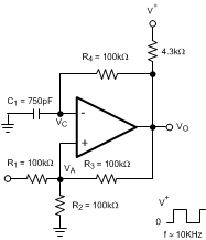 Figure 27. Square Wave Oscillator Application
8.2.1.1 Design Requirements
A typical application for a comparator is as a square wave oscillator. Figure 27 generates a square wave whose period is set by the RC time constant of the capacitor C1and resistor R4. The maximum frequency is limited by the large signal propagation delay of the comparator, and by the capacitive loading at the output, which limits the output slew rate.
8.2.1.2 Detailed Design Procedure
To analyze the circuit, consider it when the output is high. That implies that the inverted input (VC) is lower than the Non-Inverting input (VA).
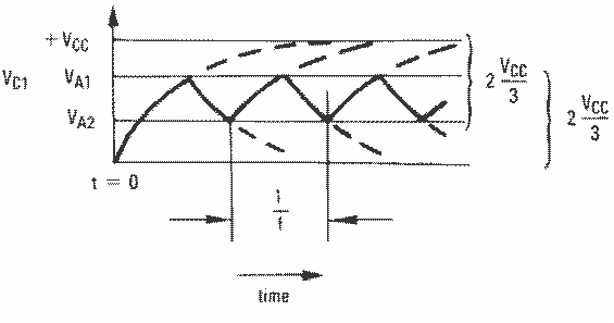 Figure 28. Squarewave Oscillator Timing Thresholds
This causes the C1 to get charged through R4, and the voltage VC increases till it is equal to the Non-Inverting input. The value of VA at this point is

If R1 = R2 = R3, then VA1 = 2VCC/3
At this point the comparator switches pulling down the output to the negative rail. The value of VA at this point is

If R1 = R2 = R3, then VA2 = VCC/3
The capacitor C1 now discharges through R4, and the voltage VC decreases till it is equal to VA2, at which point the comparator switches again, bringing it back to the initial stage. The time period is equal to twice the time it takes to discharge C1 from 2VCC/3 to VCC/3, which is given by R4C1.ln2. Hence the formula for the frequency is:
F = 1/(2·R4·C1·ln2)
8.2.1.3 Application Curve
Figure 29 shows the simulated results of an oscillator using the following values:
- R1 = R2 = R3 = R4 = 100 kΩ
- C1 = 750 pF, CL = 20 pF
- V+ = 5 V, V- = GND
- CSTRAY (not shown) from Va to GND = 10 pF
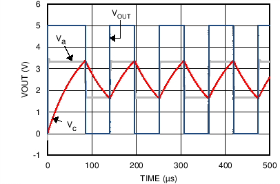 Figure 29. Square Wave Oscillator Output Waveforms
8.2.2 Positive Peak Detector
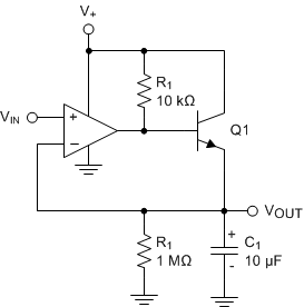 Figure 30. Positive Peak Detector
The positive peak detector is basically the comparator operated as a unity gain follower with a large holding capacitor from the output to ground. A transistor is added to the output to provide a low impedance current source. The upper output swing is limited by the emitter-base forward voltage. This allows capture of the most positive input signal between 0 V and (V+) - 0.7V.
When the output of the comparator goes high, current is passed through the transistor to charge up the capacitor. The only discharge path will be the 1-MΩ resistor shunting C1 and any load that is connected to the output. The decay time can be altered simply by changing the 1-MΩ resistor.
8.2.3 Negative Peak Detector
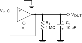 Figure 31. Negative Peak Detector for Negative Supply
The Negative Peak Detector circuit will store the peak negative voltage below ground ( 0 V to V-). For the negative detector, the output transistor acts as a low-impedance current sink.
When VIN is more negative than VOUT, the output transistor will conduct and pull the output to -VCC, charging C1. Charging stops when C1 reaches the same level as VIN. Because there is no pull-up resistor, the only discharge path will be the 1-MΩ resistor and any load impedance applied. Therefore, the decay time is set by varying the 1-MΩ resistor. Be sure to observe the polarity of C1!
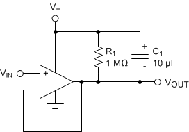 Figure 32. Negative Peak Detector for Positive Supply
An alternate positive supply version is shown in Figure 32 that will capture the lowest applied VIN value between V+ and ground (V+ to 0V).
The output of either version should be buffered by a high-impedance follower stage to prevent loading of the RC circuit.
8.2.4 Window Detector
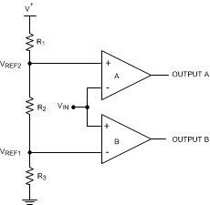 Figure 33. Window Detector
A window detector monitors the input signal to determine if it falls between two voltage levels. Both outputs are true (high) when VREF1 < VIN < VREF2
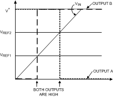 Figure 34. Window Detector Output Signal
The comparator outputs A and B are high only when VREF1 < VIN < VREF2, or within the window, where these are defined as:
To determine if the input signal falls outside of the two voltage levels, both inputs on each comparators can be reversed to invert the logic.
The outputs should be tied together and use a shared pull-up resistor for a common logic output. If individual limit outputs are needed, then each output will require it's own pull-up resistor.
Other names for window detectors are: threshold detector, level detector, and amplitude trigger or detector.