JAJSB28H May   2011  – October 2023 LMZ10501

PRODUCTION DATA  

  1.   1
  2. 特長
  3. アプリケーション
  4. 概要
  5. Revision History
  6. Pin Configuration and Functions
  7. Specifications
    1. 6.1 Absolute Maximum Ratings
    2. 6.2 ESD Ratings
    3. 6.3 Recommended Operating Conditions
    4. 6.4 Thermal Information
    5. 6.5 Electrical Characteristics
    6. 6.6 System Characteristics
    7. 6.7 Typical Characteristics
  8. Detailed Description
    1. 7.1 Overview
    2. 7.2 Functional Block Diagram
    3. 7.3 Feature Description
      1. 7.3.1 Current Limit
      2. 7.3.2 Startup Behavior and Soft Start
      3. 7.3.3 Output Short Circuit Protection
      4. 7.3.4 Thermal Overload Protection
    4. 7.4 Device Functional Modes
      1. 7.4.1 Circuit Operation
      2. 7.4.2 Input Under Voltage Detection
      3. 7.4.3 Shutdown Mode
      4. 7.4.4 EN Pin Operation
      5. 7.4.5 Internal Synchronous Rectification
      6. 7.4.6 High Duty Cycle Operation
  9. Application and Implementation
    1. 8.1 Application Information
    2. 8.2 Typical Application
      1. 8.2.1 Design Requirements
      2. 8.2.2 Detailed Design Procedure
        1. 8.2.2.1 Custom Design With WEBENCH® Tools
        2. 8.2.2.2 Setting The Output Voltage
          1. 8.2.2.2.1 RT And RB Selection For Fixed VOUT
          2. 8.2.2.2.2 Output Voltage Accuracy Optimization
        3. 8.2.2.3 Dynamic Output Voltage Scaling
        4. 8.2.2.4 Integrated Inductor
        5. 8.2.2.5 Input And Output Capacitor Selection
      3. 8.2.3 Application Curves
        1. 8.2.3.1 VOUT = 1.2 V
        2. 8.2.3.2 VOUT = 1.8 V
        3. 8.2.3.3 VOUT = 2.5 V
        4. 8.2.3.4 VOUT = 3.3 V
    3. 8.3 Power Supply Recommendations
      1. 8.3.1 Voltage Range
      2. 8.3.2 Current Capability
      3. 8.3.3 Input Connection
        1. 8.3.3.1 Voltage Drops
        2. 8.3.3.2 Stability
    4. 8.4 Layout
      1. 8.4.1 Layout Guidelines
      2. 8.4.2 Layout Example
      3. 8.4.3 Package Considerations
  10. Device and Documentation Support
    1. 9.1 Device Support
      1. 9.1.1 Custom Design With WEBENCH® Tools
    2. 9.2 Documentation Support
      1. 9.2.1 Related Documentation
    3. 9.3 ドキュメントの更新通知を受け取る方法
    4. 9.4 サポート・リソース
    5. 9.5 Trademarks
    6. 9.6 静電気放電に関する注意事項
    7. 9.7 用語集
  11. 10Mechanical, Packaging, and Orderable Information

パッケージ・オプション

デバイスごとのパッケージ図は、PDF版データシートをご参照ください。

メカニカル・データ(パッケージ|ピン)
  • SIL|8
サーマルパッド・メカニカル・データ
発注情報

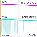
High Duty Cycle Operation

The LMZ10501 features a transition mode designed to extend the output regulation range to the minimum possible input voltage. As the input voltage decreases closer and closer to VOUT, the off-time of the PFET gets smaller and smaller and the duty cycle eventually must reach 100% to support the output voltage. The input voltage at which the duty cycle reaches 100% is the edge of regulation. When the LMZ10501 input voltage is lowered, such that the off-time of the PFET reduces to less than 35ns, the LMZ10501 doubles the switching period to extend the off-time for that VIN and maintain regulation. If VIN is lowered even more, the off-time of the PFET will reach the 35ns mark again. The LMZ10501 will then reduce the frequency again, achieving less than 100% duty cycle operation and maintaining regulation. As VIN is lowered even more, the LMZ10501 will continue to scale down the frequency, aiming to maintain at least 35ns off time. Eventually, as the input voltage decreases further, 100% duty cycle is reached. This behavior of extending the VIN regulation range is illustrated in Figure 7-3.
GUID-6300E819-7E74-40B2-A3AA-CBC07F50EA8A-low.gifFigure 7-3 High Duty Cycle Operation and Switching Frequency Reduction