JAJSH78J June 2010 – April 2019 LMZ10503EXT
PRODUCTION DATA.
- 1 特長
- 2 アプリケーション
- 3 概要
- 4 改訂履歴
- 5 概要(続き)
- 6 Pin Configuration and Functions
- 7 Specifications
- 8 Detailed Description
- 9 Application and Implementation
- 10Power Supply Recommendations
- 11Layout
- 12デバイスおよびドキュメントのサポート
- 13メカニカル、パッケージ、および注文情報
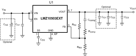
9.3.1 Application Schematic for 3.3-V to 5-V Input and 2.5-V Output With Optimized Ripple and Transient Response
The compensation for each solution was optimized to work over the full input range. Many applications have a fixed input voltage rail. It is possible to modify the compensation to obtain a faster transient response for a given input voltage operating point.
 Figure 26. Schematic for 2.5-V Output Based on 3.3-V to 5-V Input
 Table 5. Bill of Materials, VIN = 3.3 V to 5 V, VOUT = 2.5 V, IOUT (MAX) = 3 A,
Optimized for Low Input and Output Ripple Voltage and Fast Transient Response
| DESIGNATOR | DESCRIPTION | CASE SIZE | MANUFACTURER | MANUFACTURER P/N | QUANTITY |
|---|---|---|---|---|---|
| U1 | Power module | PFM-7 | Texas Instruments | LMZ10503EXTTZ-ADJ | 1 |
| Cin1 | 22 µF, X5R, 10 V | 1210 | AVX | 1210ZD226MAT | 2 |
| Cin2 | 220 µF, 10 V, AL-Elec | E | Panasonic | EEE1AA221AP | 1(1) |
| CO1 | 4.7 µF, X5R, 10 V | 0805 | AVX | 0805ZD475MAT | 1(1) |
| CO2 | 22 µF, X5R, 6.3 V | 1206 | AVX | 12066D226MAT | 1(1) |
| CO3 | 100 µF, X5R, 6.3 V | 1812 | AVX | 18126D107MAT | 1 |
| Rfbt | 75 kΩ | 0402 | Vishay Dale | CRCW040275K0FKED | 1 |
| Rfbb | 34.8 kΩ | 0402 | Vishay Dale | CRCW040234K8FKED | 1 |
| Rcomp | 1.0 kΩ | 0402 | Vishay Dale | CRCW04021K00FKED | 1 |
| Ccomp | 220 pF, ±5%, C0G, 50 V | 0402 | Murata | GRM1555C1H221JA01D | 1 |
| CSS | 10 nF, ±10%, X7R, 16 V | 0402 | Murata | GRM155R71C103KA01 | 1 |
(1) Optional components, include for low input and output voltage ripple.
Table 6. Output Voltage Setting (Rfbt = 75 kΩ)
| VOUT | Rfbb |
|---|---|
| 3.3V | 23.7 kΩ |
| 2.5 V | 34.8 kΩ |
| 1.8 V | 59 kΩ |
| 1.5 V | 84.5 kΩ |
| 1.2 V | 150 kΩ |
| 0.9 V | 590 kΩ |