JAJSH79J June   2010  – April 2019 LMZ10504EXT

PRODUCTION DATA.  

  1. 特長
  2. アプリケーション
  3. 概要
    1.     Device Images
      1.      代表的なアプリケーション回路
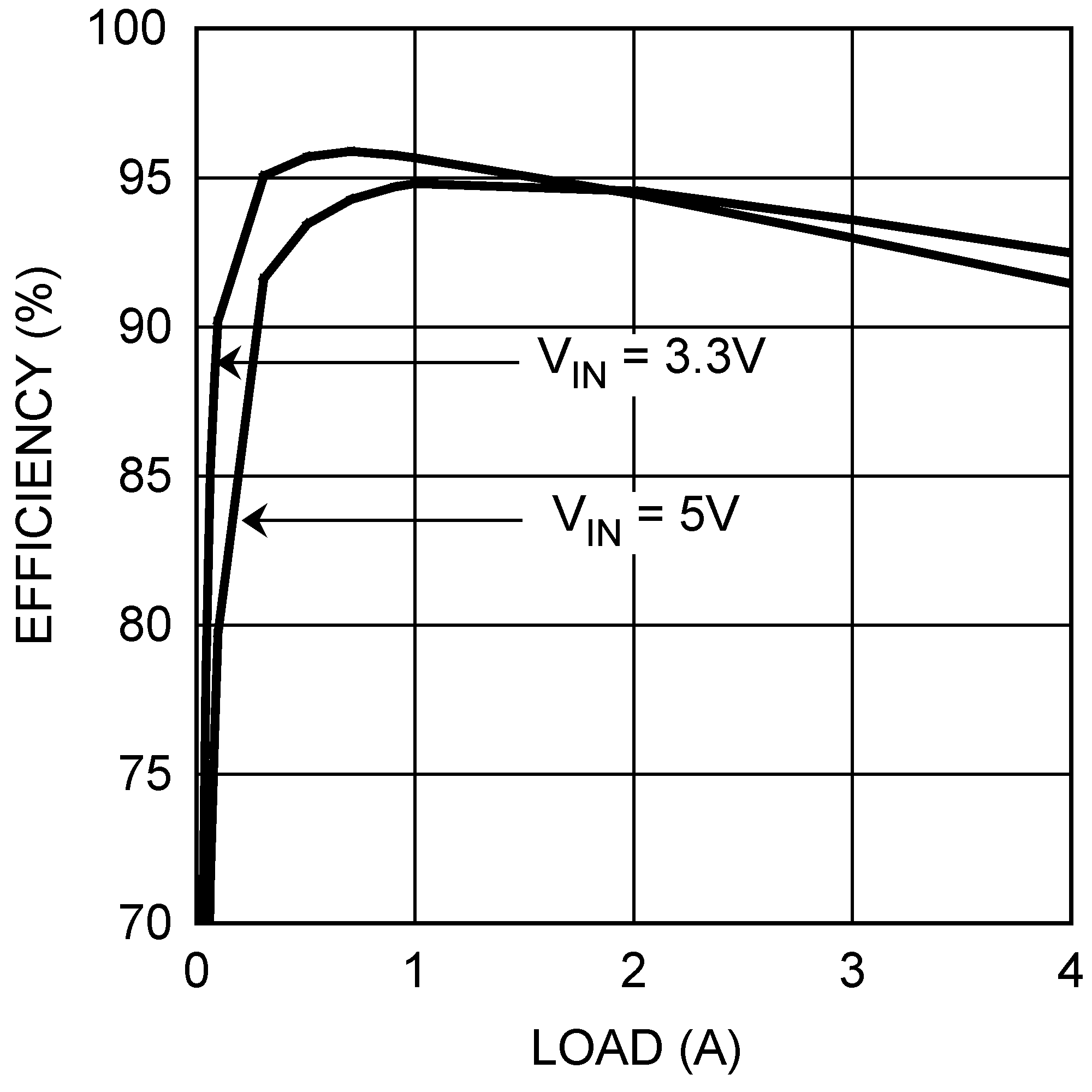
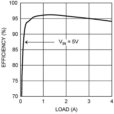
      2.      VOUT = 3.3Vでの効率
  4. 改訂履歴
  5. 概要(続き)
  6. Pin Configuration and Functions
    1.     Pin Functions
  7. Specifications
    1. 7.1 Absolute Maximum Ratings
    2. 7.2 ESD Ratings
    3. 7.3 Recommended Operating Conditions
    4. 7.4 Thermal Information
    5. 7.5 Electrical Characteristics
    6. 7.6 Typical Characteristics
  8. Detailed Description
    1. 8.1 Overview
    2. 8.2 Functional Block Diagram
    3. 8.3 Feature Description
      1. 8.3.1 Enable
      2. 8.3.2 Enable and UVLO
      3. 8.3.3 Soft-Start
      4. 8.3.4 Soft-Start Capacitor
      5. 8.3.5 Tracking
      6. 8.3.6 Tracking - Equal Soft-Start Time
      7. 8.3.7 Tracking - Equal Slew Rates
      8. 8.3.8 Current Limit
      9. 8.3.9 Overtemperature Protection
    4. 8.4 Device Functional Modes
      1. 8.4.1 Prebias Start-Up Capability
  9. Application and Implementation
    1. 9.1 Application Information
    2. 9.2 Typical Application
      1. 9.2.1 Design Requirements
      2. 9.2.2 Detailed Design Procedure
        1. 9.2.2.1 Custom Design With WEBENCH® Tools
        2. 9.2.2.2 Input Capacitor Selection
        3. 9.2.2.3 Output Capacitor Selection
          1. 9.2.2.3.1 Output Voltage Setting
        4. 9.2.2.4 Loop Compensation
      3. 9.2.3 Application Curves
    3. 9.3 System Examples
      1. 9.3.1 Application Schematic for 3.3-V to 5-V Input and 2.5-V Output With Optimized Ripple and Transient Response
      2. 9.3.2 Application Schematic for 3.3-V to 5-V Input and 2.5-V Output
      3. 9.3.3 EMI Tested Schematic for 2.5-V Output Based on 3.3-V to 5-V Input
  10. 10Power Supply Recommendations
  11. 11Layout
    1. 11.1 Layout Guidelines
    2. 11.2 Layout Examples
    3. 11.3 Estimate Power Dissipation and Thermal Considerations
    4. 11.4 Power Module SMT Guidelines
  12. 12デバイスおよびドキュメントのサポート
    1. 12.1 デバイス・サポート
      1. 12.1.1 デベロッパー・ネットワークの製品に関する免責事項
      2. 12.1.2 開発サポート
        1. 12.1.2.1 WEBENCH®ツールによるカスタム設計
    2. 12.2 ドキュメントのサポート
      1. 12.2.1 関連資料
    3. 12.3 ドキュメントの更新通知を受け取る方法
    4. 12.4 コミュニティ・リソース
    5. 12.5 商標
    6. 12.6 静電気放電に関する注意事項
    7. 12.7 Glossary
  13. 13メカニカル、パッケージ、および注文情報

パッケージ・オプション

メカニカル・データ(パッケージ|ピン)
サーマルパッド・メカニカル・データ
発注情報

Typical Characteristics

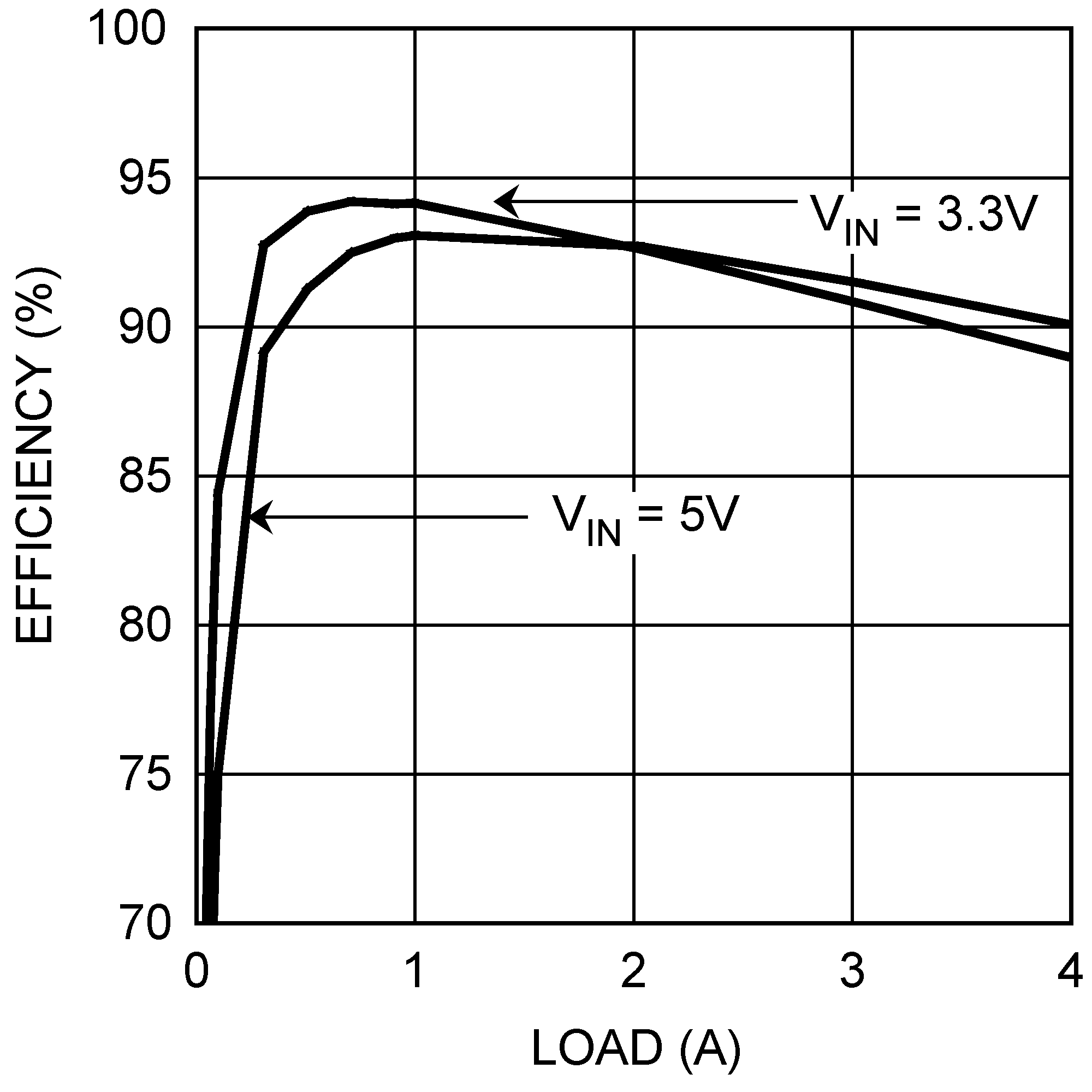
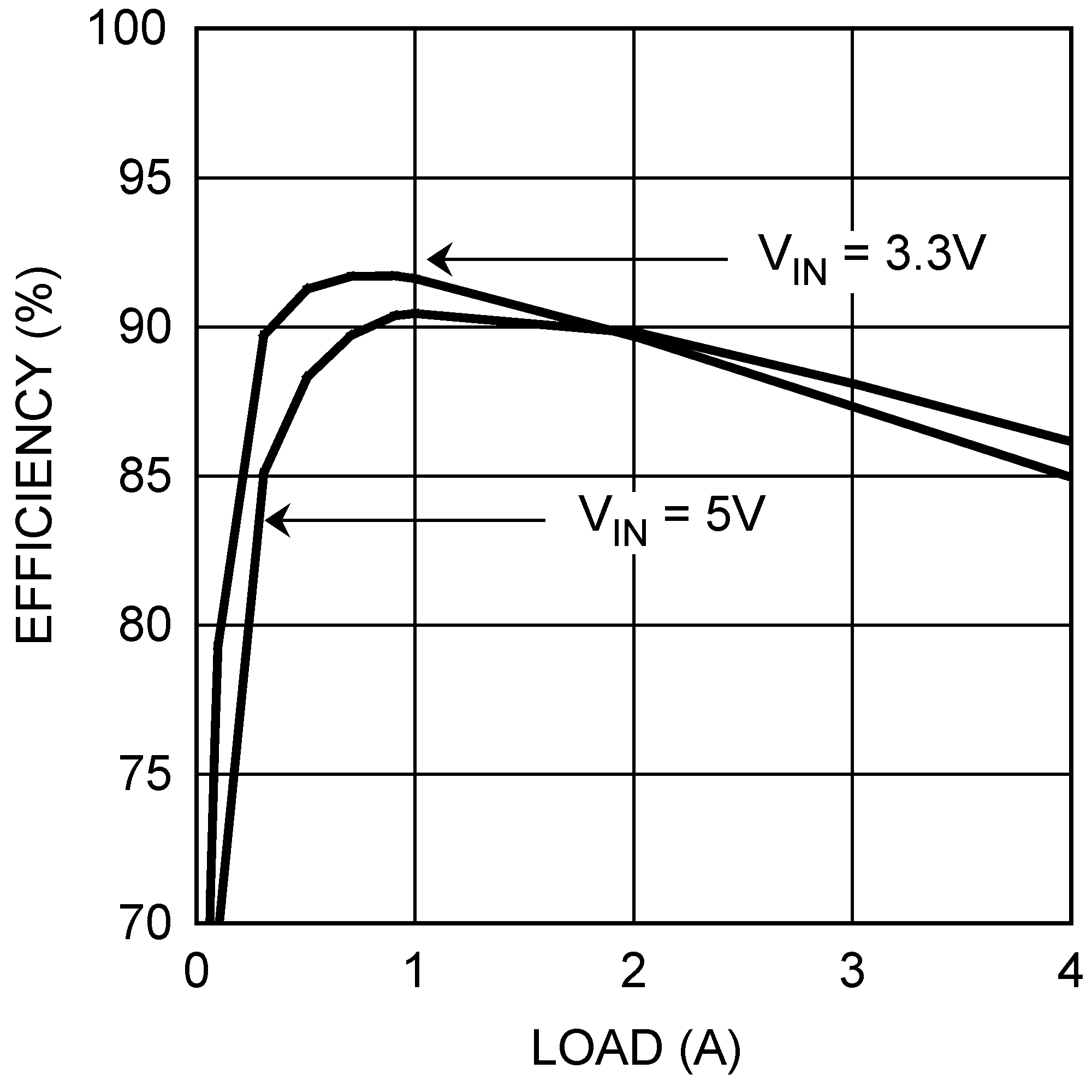
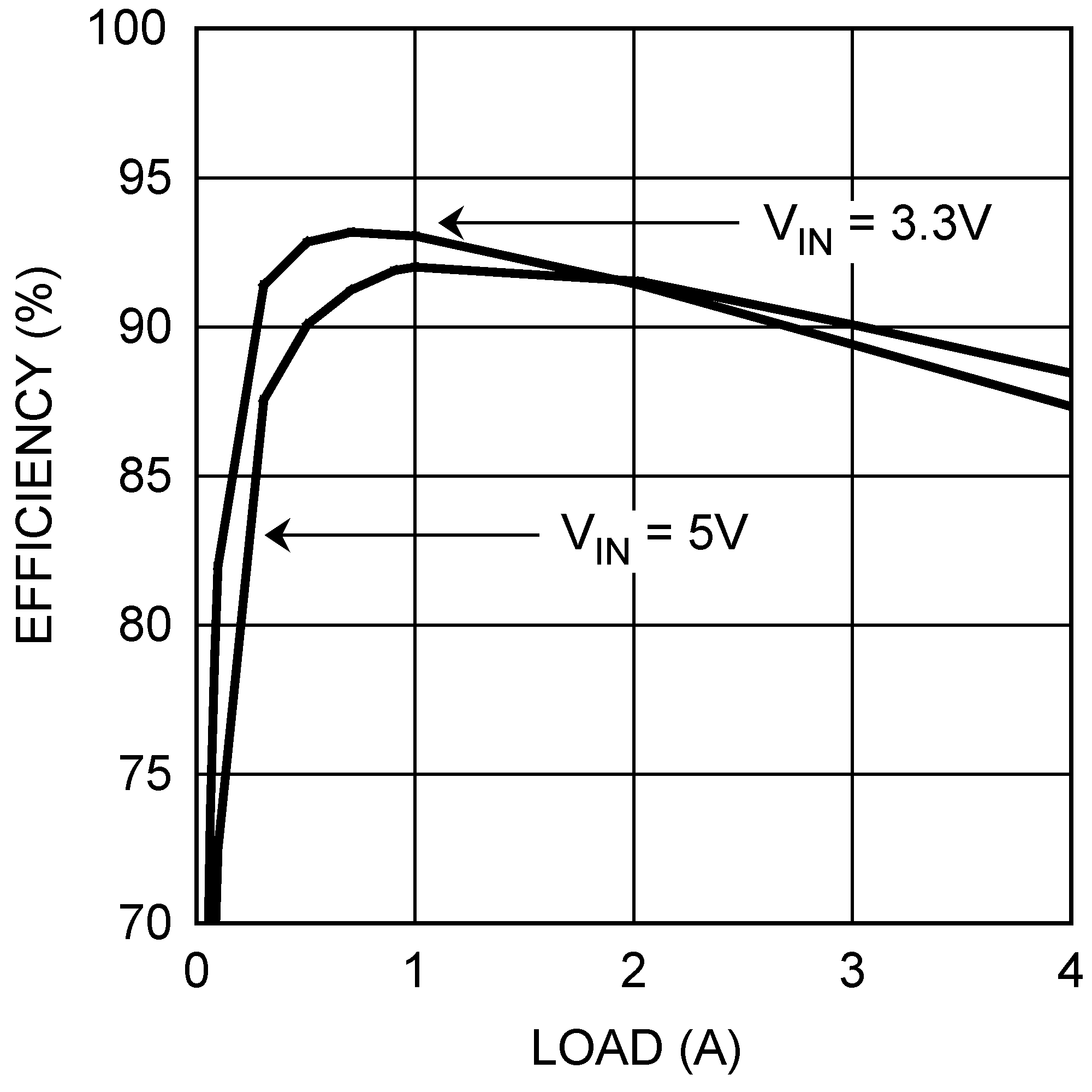
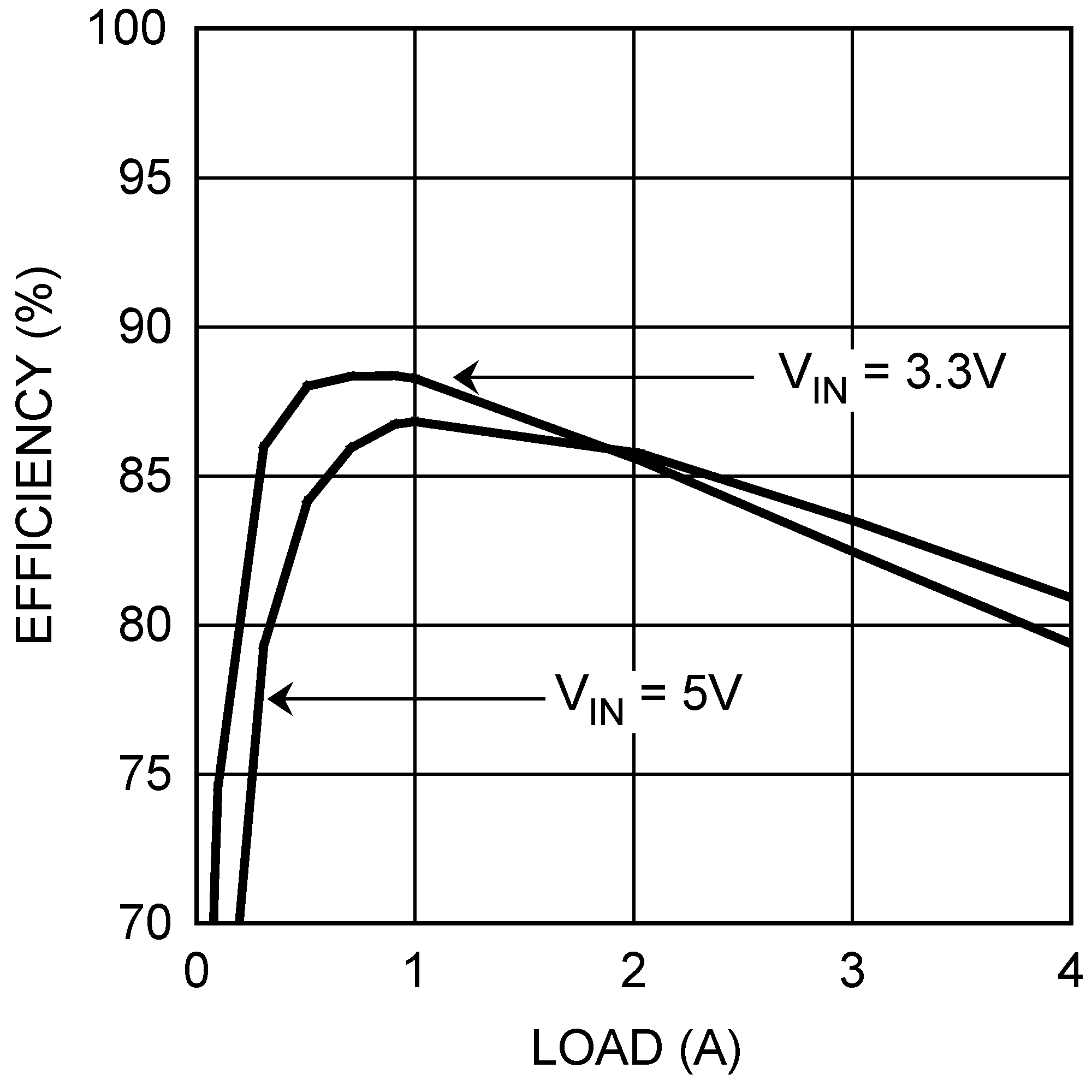
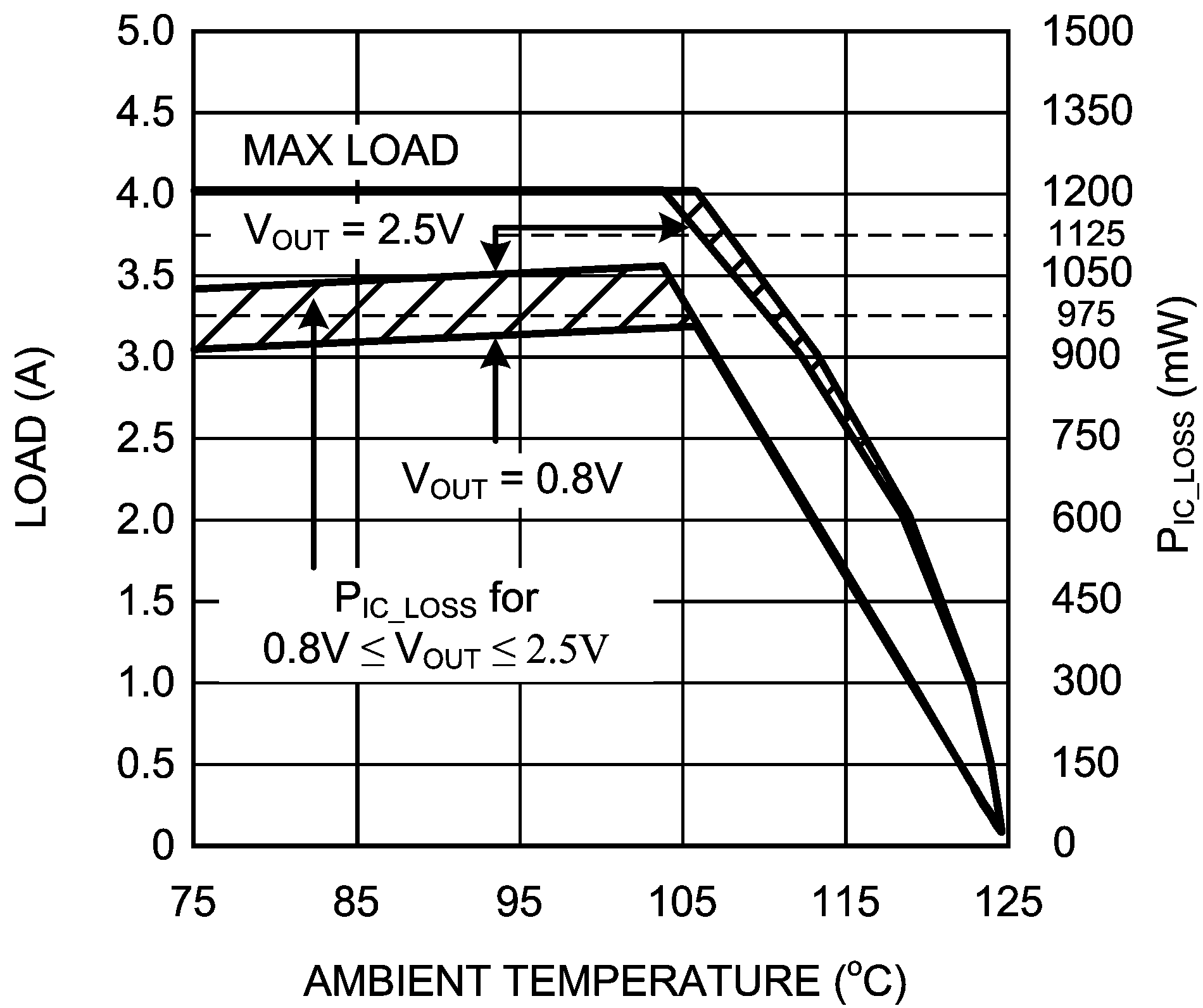
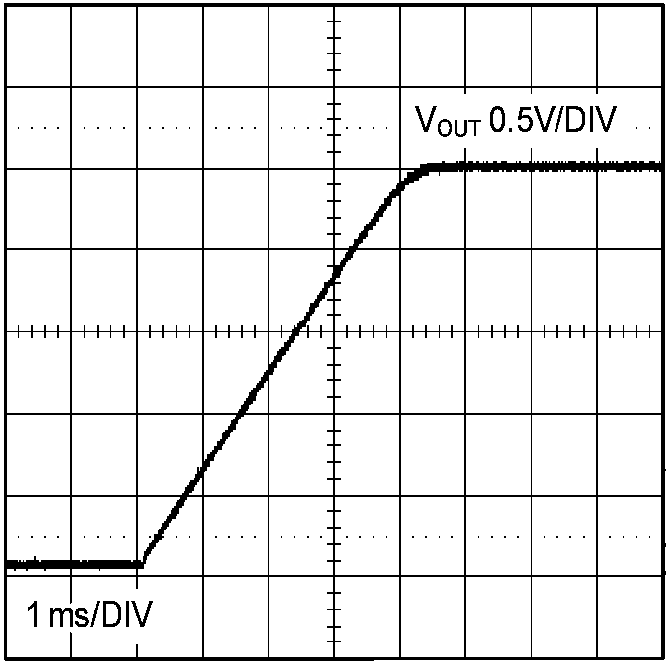
Unless otherwise specified, the following conditions apply: VIN = VEN = 5 V, CIN is 47-µF 10-V X5R ceramic capacitor; TAMBIENT = 25°C for efficiency curves and waveforms.
LMZ10504EXT 30118471.png
VOUT = 3.3 V
Figure 1. Efficiency
LMZ10504EXT 30118469.png
VOUT = 1.8 V
Figure 3. Efficiency
LMZ10504EXT 30118468.png
VOUT = 1.2 V
Figure 5. Efficiency
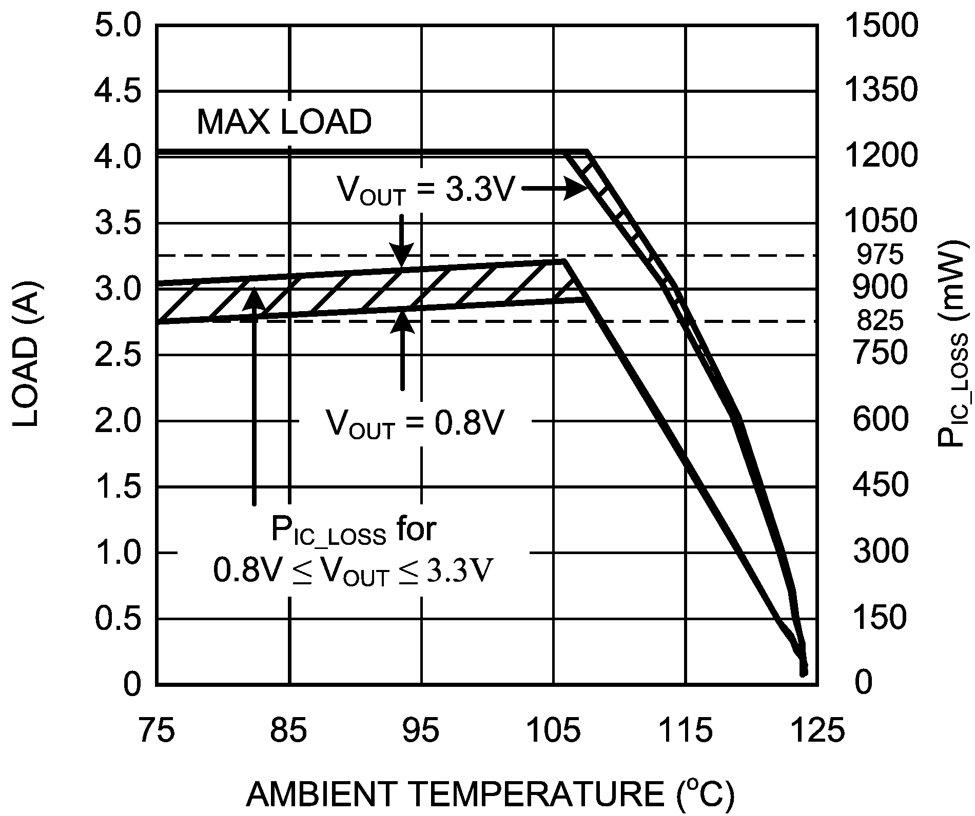
LMZ10504EXT 30118410.png
VIN = 5 V, RθJA = 20°C/W
Figure 7. Current Derating
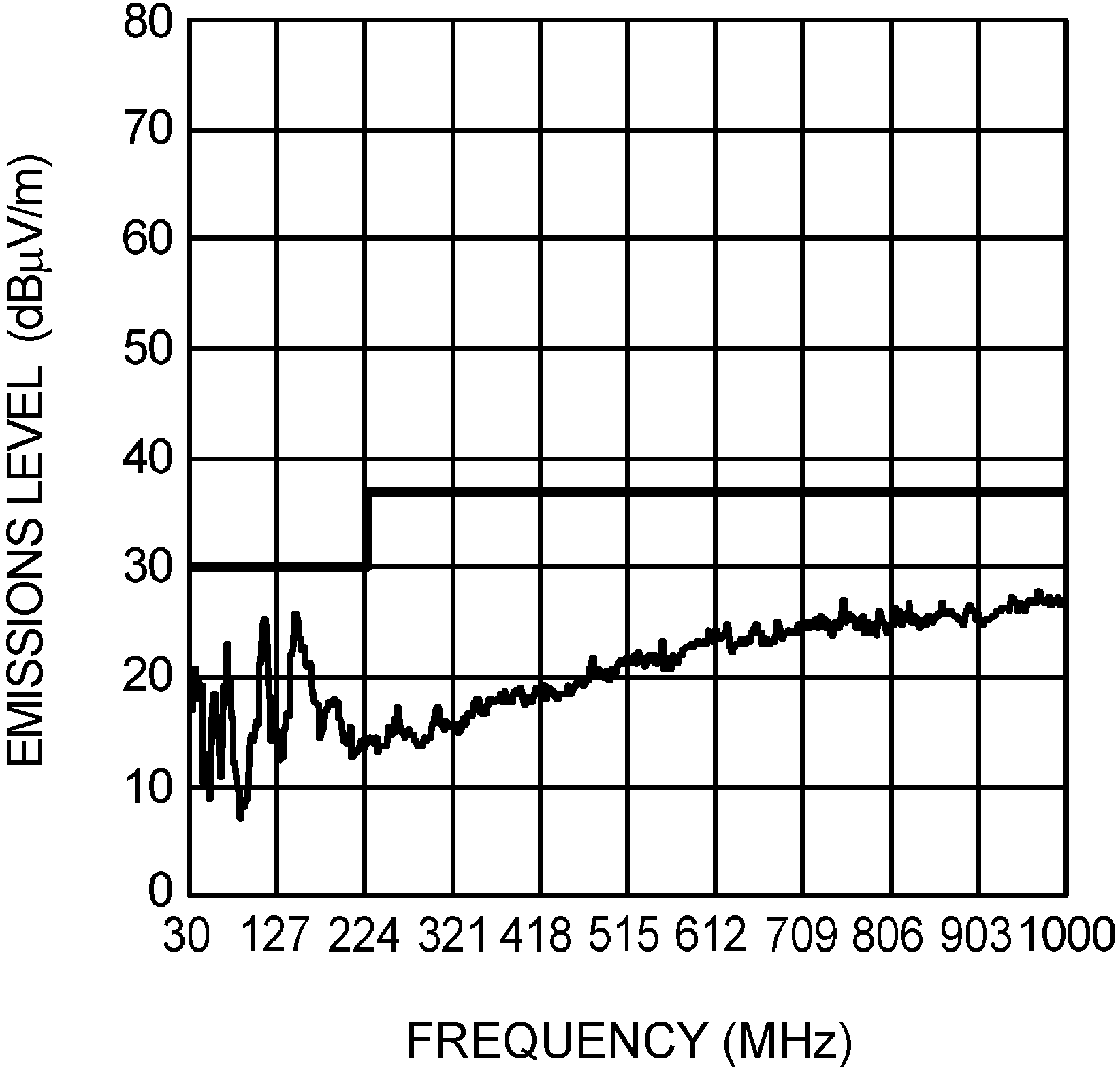
LMZ10504EXT 30118499.png
VIN = 5 V, VOUT = 2.5 V, IOUT = 4 A
Evaluation Board
Figure 9. Radiated Emissions (EN 55022, Class B)
LMZ10504EXT 30118455.png
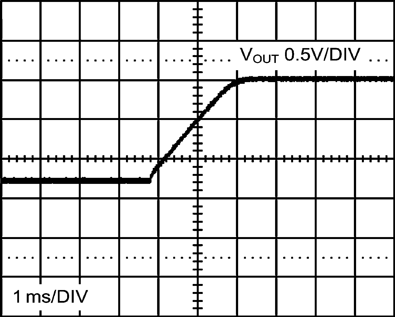
VOUT = 2.5 V, IOUT = 0 A
Figure 11. Prebiased Start-Up
LMZ10504EXT 30118463.png
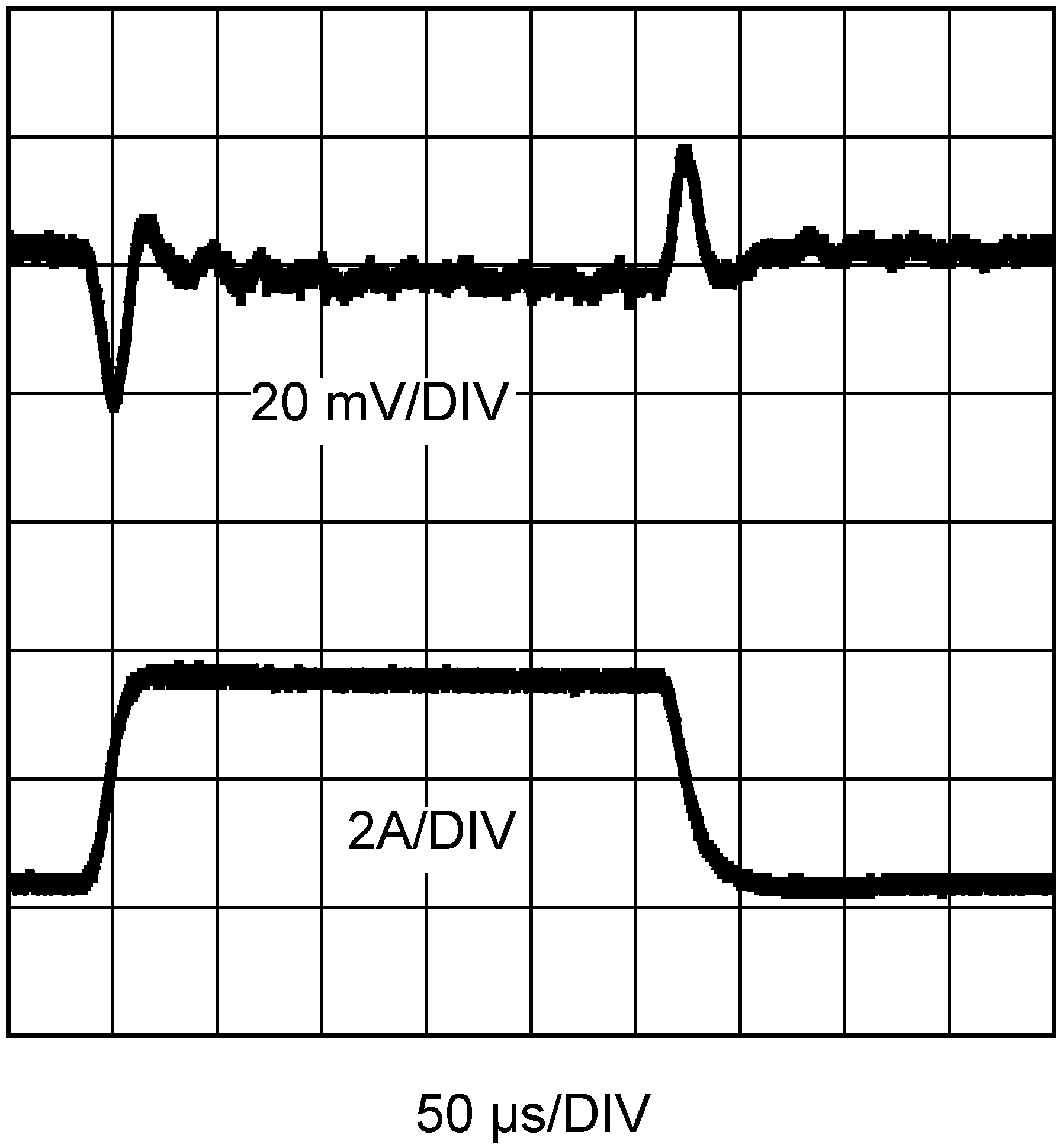
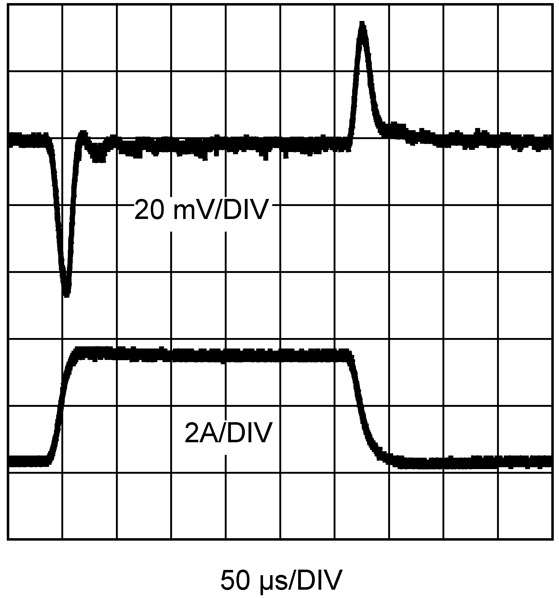
VIN = 5.0 V, VOUT = 2.5 V, IOUT = 0.4-A to 3.6-A to 0.4-A Step
20 mV/DIV, 20-MHz Bandwidth Limited
Refer to Table 5 for BOM, includes optional components
Figure 13. Load Transient Response
LMZ10504EXT 30118465.png
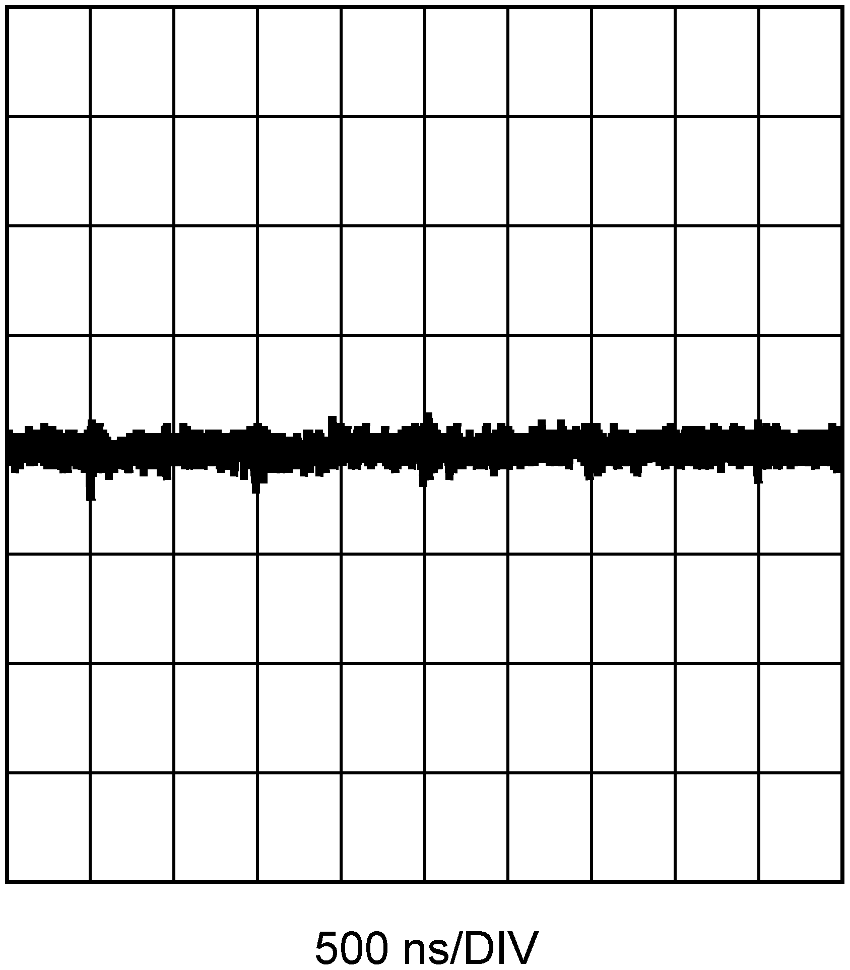
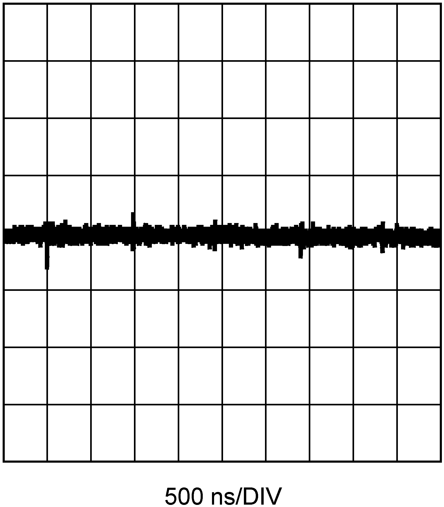
VIN = 5.0 V, VOUT = 2.5 V, IOUT = 4 A,
20 mV/DIV. Refer to Table 5 for BOM
Figure 15. Output Voltage Ripple
LMZ10504EXT 30118470.png
VOUT = 2.5 V
Figure 2. Efficiency
LMZ10504EXT 30118402.png
VOUT = 1.5 V
Figure 4. Efficiency
LMZ10504EXT 30118467.png
VOUT = 0.8 V
Figure 6. Efficiency
LMZ10504EXT 30118411.png
VIN = 3.3 V, RθJA = 20°C/W
Figure 8. Current Derating
LMZ10504EXT 30118456.png
VOUT = 2.5 V, IOUT = 0 A
Figure 10. Start-Up
LMZ10504EXT 30118462.png
VIN = 3.3 V, VOUT = 2.5 V, IOUT = 0.4-A to 3.6-A to 0.4-A Step
20 mV/DIV, 20-MHz Bandwidth Limited
Refer to Table 5 for BOM, includes optional components
Figure 12. Load Transient Response
LMZ10504EXT 30118464.png
VIN = 3.3 V, VOUT = 2.5 V, IOUT = 4 A, 20 mV/DIV
Refer to Table 5 for BOM
Figure 14. Output Voltage Ripple