JAJSF82E June 2013 – February 2020 LMZ31704
PRODUCTION DATA.
- 1 特長
- 2 アプリケーション
- 3 概要
- 4 改訂履歴
- 5 Specifications
- 6 Device Information
- 7 Typical Characteristics (PVIN = VIN = 12 V)
- 8 Typical Characteristics (PVIN = VIN = 5 V)
- 9 Typical Characteristics (PVIN = 3.3 V, VIN = 5 V)
-
10Application Information
- 10.1 Adjusting the Output Voltage
- 10.2 Capacitor Recommendations for the LMZ31704 Power Supply
- 10.3 Transient Response
- 10.4 Transient Waveforms
- 10.5 Application Schematics
- 10.6 Custom Design With WEBENCH® Tools
- 10.7 VIN and PVIN Input Voltage
- 10.8 3.3 V PVIN Operation
- 10.9 Power Good (PWRGD)
- 10.10 SYNC_OUT
- 10.11 Parallel Operation
- 10.12 Light Load Efficiency (LLE)
- 10.13 Power-Up Characteristics
- 10.14 Pre-Biased Start-up
- 10.15 Remote Sense
- 10.16 Thermal Shutdown
- 10.17 Output On/Off Inhibit (INH)
- 10.18 Slow Start (SS/TR)
- 10.19 Overcurrent Protection
- 10.20 Synchronization (CLK)
- 10.21 Sequencing (SS/TR)
- 10.22 Programmable Undervoltage Lockout (UVLO)
- 10.23 Layout Considerations
- 10.24 EMI
- 11デバイスおよびドキュメントのサポート
- 12メカニカル、パッケージ、および注文情報
10.23 Layout Considerations
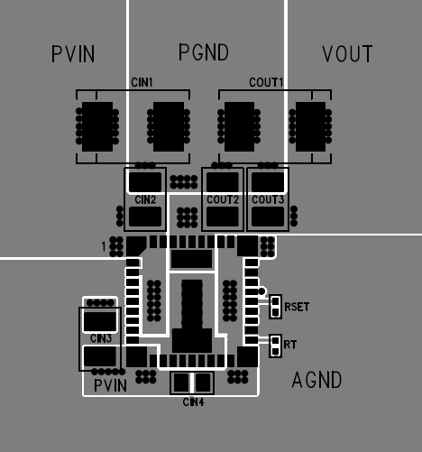
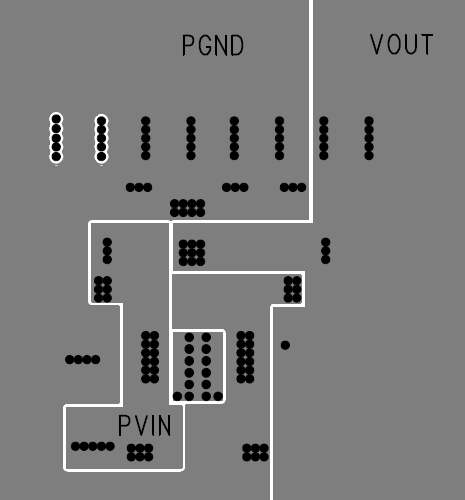
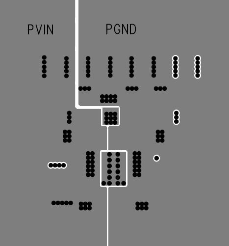
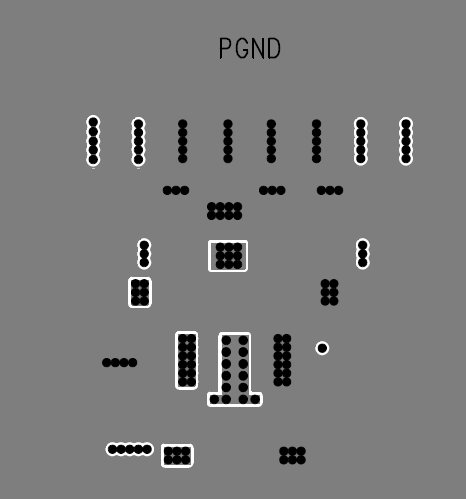
To achieve optimal electrical and thermal performance, an optimized PCB layout is required. Figure 42 through Figure 45 shows a typical PCB layout. Some considerations for an optimized layout are:
- Use large copper areas for power planes (PVIN, VOUT, and PGND) to minimize conduction loss and thermal stress.
- Place ceramic input and output capacitors close to the device pins to minimize high frequency noise.
- Locate additional output capacitors between the ceramic capacitor and the load.
- Keep AGND and PGND separate from one another.
- Place RSET, RRT, and CSS as close as possible to their respective pins.
- Use multiple vias to connect the power planes to internal layers.
 Figure 42. Typical Top-Layer Layout
  Figure 44. Typical Layer-3 Layout
  Figure 43. Typical Layer-2 Layout
  Figure 45. Typical Bottom-Layer Layout