SNOSCX9A March 2015 – November 2015 LPV542
PRODUCTION DATA.
- 1 Features
- 2 Applications
- 3 Description
- 4 Revision History
- 5 Pin Configuration and Functions
- 6 Specifications
- 7 Detailed Description
- 8 Application and Implementation
- 9 Power Supply Recommendations
- 10Layout
- 11Device and Documentation Support
- 12Mechanical, Packaging, and Orderable Information
パッケージ・オプション
メカニカル・データ(パッケージ|ピン)
サーマルパッド・メカニカル・データ
- DGK|8
発注情報
7 Detailed Description
7.1 Overview
The LPV542 dual op amplifier is unity-gain stable and can operate on a single supply, making it highly versatile and easy to use.
The LPV542 is fully specified and tested from 1.6 V to 5.5 V. Parameters that vary significantly with operating voltages or temperature are shown in the Typical Characteristics curves.
7.2 Functional Block Diagram

7.3 Feature Description
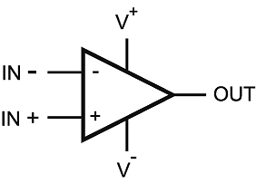
The amplifier's differential inputs consist of a non-inverting input (+IN) and an inverting input (–IN). The amplifer amplifies only the difference in voltage between the two inputs, which is called the differential input voltage. The output voltage of the op-amp VOUT is given by Equation 1:
where
- AOL is the open-loop gain of the amplifier, typically around 100 dB (100,000x, or 100,000 Volts per microvolt).
7.4 Device Functional Modes
7.4.1 Rail-To-Rail Input
The input common-mode voltage range of the LPV542 extends to the supply rails. This is achieved with a complementary input stage — an N-channel input differential pair in parallel with a P-channel differential pair. The N-channel pair is active for input voltages close to the positive rail, typically (V+) – 800 mV to 200 mV above the positive supply, while the P-channel pair is on for inputs from 300 mV below the negative supply to approximately (V+) – 800 mV. There is a small transition region, typically (V+) – 1.2 V to (V+) – 0.8 V, in which both pairs are on. This 400 mV transition region can vary 200 mV with process variation. Within the 400 mV transition region PSRR, CMRR, offset voltage, offset drift, and THD may be degraded compared to operation outside this region.
7.4.2 Supply Current Changes over Common Mode
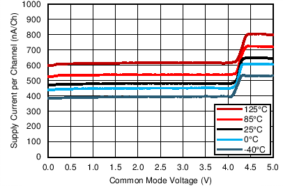
Because of the ultra-low supply current, changes in common mode voltages will cause a noticeable change in the supply current as the input stages transition through the transition region, as shown in Figure 37 below.
 Figure 37. Supply Current Change over Common Mode at 5 V
For the lowest supply current operation, keep the input common mode range between V- and 1 V below V+.
7.4.3 Design Optimization With Rail-To-Rail Input
In most applications, operation is within the range of only one differential pair. However, some applications can subject the amplifier to a common-mode signal in the transition region. Under this condition, the inherent mismatch between the two differential pairs may lead to degradation of the CMRR and THD. The unity-gain buffer configuration is the most problematic as it will traverse through the transition region if a sufficiently wide input swing is required.
7.4.4 Design Optimization for Nanopower Operation
When designing for ultralow power, choose system components carefully. To minimize current consumption, select large-value resistors. Any resistors will react with stray capacitance in the circuit and the input capacitance of the operational amplifier. These parasitic RC combinations can affect the stability of the overall system. A feedback capacitor may be required to assure stability and limit overshoot or gain peaking.
When possible, use AC coupling and AC feedback to reduce static current draw through the feedback elements. Use film or ceramic capacitors since large electolytics may have static leakage currents in the tens to hundreds of nanoamps.
7.4.5 Common-Mode Rejection
The CMRR for the LPV542 is specified in two ways so the best match for a given application may be used. First, the CMRR of the device in the common-mode range below the transition region (VCM < (V+) – 0.9 V) is given. This specification is the best indicator of the capability of the device when the application requires use of one of the differential input pairs. Second, the CMRR at VS = 5 V over the entire common-mode range is specified.
7.4.6 Output Stage
The LPV542 output voltage swings 3 mV from rails at 3.3 V supply, which provides the maximum possible dynamic range at the output. This is particularly important when operating on low supply voltages.
The LPV542 Maximum Output Voltage Swing defines the maximum swing possible under a particular output load.
7.4.7 Driving Capacitive Load
The LPV542 is internally compensated for stable unity gain operation, with a 8 kHz typical gain bandwidth. However, the unity gain follower is the most sensitive configuration to capacitive load. The combination of a capacitive load placed directly on the output of an amplifier along with the amplifier’s output impedance creates a phase lag, which reduces the phase margin of the amplifier. If the phase margin is significantly reduced, the response will be under damped which causes peaking in the transfer and, when there is too much peaking, the op amp might start oscillating.
In order to drive heavy (>50pF) capacitive loads, an isolation resistor, RISO, should be used, as shown in Figure 38. By using this isolation resistor, the capacitive load is isolated from the amplifier’s output. The larger the value of RISO, the more stable the amplifier will be. If the value of RISO is sufficiently large, the feedback loop will be stable, independent of the value of CL. However, larger values of RISO result in reduced output swing and reduced output current drive.
 Figure 38. Resistive Isolation Of Capacitive Load