JAJSGG7B January 2019 – August 2019 OPA1671
PRODUCTION DATA.
- 1 特長
- 2 アプリケーション
- 3 概要
- 4 改訂履歴
- 5 Pin Configuration and Functions
- 6 Specifications
- 7 Detailed Description
- 8 Application and Implementation
- 9 Power Supply Recommendations
- 10Layout
- 11デバイスおよびドキュメントのサポート
- 12メカニカル、パッケージ、および注文情報
パッケージ・オプション
メカニカル・データ(パッケージ|ピン)
サーマルパッド・メカニカル・データ
発注情報
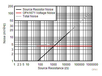
8.1.2 Noise Performance
Figure 31 shows the total circuit noise for varying source impedances with the operational amplifier in a unity-gain configuration (with no feedback resistor network and therefore no additional noise contributions). The op amp itself contributes a voltage noise component and a current noise component. The voltage noise is commonly modeled as a time-varying component of the offset voltage. The current noise is modeled as the time-varying component of the input bias current and reacts with the source resistance to create a voltage component of noise. For a CMOS-input device, the noise resulting from the input current is negligible; therefore, the total noise is dominated by the voltage noise of the OPA1671 at low source resistance, and the resistor noise > 1 kΩ.
Figure 31 shows the calculation of the total circuit noise, with these parameters:
- en = voltage noise
- RS = source impedance
- k = Boltzmann's constant = 1.38 × 10⁻²³ J/K
- T = temperature in kelvins (K)
For more details on calculating noise, see Basic Noise Calculations.
 Figure 32. Noise Performance of the OPA1671 in a Unity-Gain Buffer Configuration