JAJSGR4B September   2014  – December 2018 OPA2320-Q1 , OPA320-Q1

PRODUCTION DATA.  

  1. 特長
  2. アプリケーション
    1.     ゼロ・クロスオーバー歪み:低オフセット電圧
  3. 概要
  4. 改訂履歴
  5. Pin Configuration and Functions
    1.     Pin Functions
  6. Specifications
    1. 6.1 Absolute Maximum Ratings
    2. 6.2 ESD Ratings
    3. 6.3 Recommended Operating Conditions
    4. 6.4 Thermal Information
    5. 6.5 Electrical Characteristics:
    6. 6.6 Typical Characteristics
  7. Detailed Description
    1. 7.1 Overview
    2. 7.2 Functional Block Diagram
    3. 7.3 Feature Description
      1. 7.3.1 Input and ESD Protection
      2. 7.3.2 Feedback Capacitor Improves Response
      3. 7.3.3 EMI Susceptibility And Input Filtering
      4. 7.3.4 Output Impedance
      5. 7.3.5 Capacitive Load and Stability
      6. 7.3.6 Overload Recovery Time
    4. 7.4 Device Functional Modes
      1. 7.4.1 Rail-to-Rail Input
      2. 7.4.2 Phase Reversal
  8. Application and Implementation
    1. 8.1 Application Information
    2. 8.2 Typical Applications
      1. 8.2.1 Transimpedance Amplifier
        1. 8.2.1.1 Design Requirements
        2. 8.2.1.2 Detailed Design Procedure
          1. 8.2.1.2.1 Optimizing The Transimpedance Circuit
        3. 8.2.1.3 Application Curves
      2. 8.2.2 High-Impedance Sensor Interface
      3. 8.2.3 Driving ADCs
      4. 8.2.4 Active Filter
  9. Power Supply Recommendations
  10. 10Layout
    1. 10.1 Layout Guidelines
    2. 10.2 Layout Example
  11. 11デバイスおよびドキュメントのサポート
    1. 11.1 デバイス・サポート
      1. 11.1.1 開発サポート
    2. 11.2 関連リンク
    3. 11.3 ドキュメントの更新通知を受け取る方法
    4. 11.4 コミュニティ・リソース
    5. 11.5 商標
    6. 11.6 静電気放電に関する注意事項
    7. 11.7 Glossary
  12. 12メカニカル、パッケージ、および注文情報

パッケージ・オプション

メカニカル・データ(パッケージ|ピン)
サーマルパッド・メカニカル・データ
発注情報

Overload Recovery Time

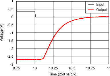
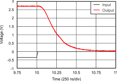
Overload recovery time is the time it takes the output of the amplifier to come out of saturation and recover to the linear region. Overload recovery is particularly important in applications where small signals must be amplified in the presence of large transients. Figure 33 and Figure 34 show the positive and negative overload recovery times of the OPAx320-Q1, respectively. In both cases, the time elapsed before the OPAx320-Q1 come out of saturation is less than 100 ns. In addition, the symmetry between the positive and negative recovery times allows excellent signal rectification without distortion of the output signal.
OPA320-Q1 OPA2320-Q1 ai_pos_oload_recov_slos884.gif
VS = ±2.75 V, G = –10 V/V
Figure 33. Positive Recovery Time
OPA320-Q1 OPA2320-Q1 ai_neg_oload_recov_slos884.gif
VS = ±2.75 V, G = –10 V/V
Figure 34. Negative Recovery Time