JAJSFB4F September 2010 – April 2018 OPA171 , OPA2171 , OPA4171
PRODUCTION DATA.
- 1 特長
- 2 アプリケーション
- 3 概要
- 4 改訂履歴
- 5 Pin Configuration and Functions
- 6 Specifications
- 7 Detailed Description
- 8 Application and Implementation
- 9 Power Supply Recommendations
- 10Layout
- 11デバイスおよびドキュメントのサポート
- 12メカニカル、パッケージ、および注文情報
パッケージ・オプション
メカニカル・データ(パッケージ|ピン)
サーマルパッド・メカニカル・データ
発注情報
7.3.4 Capacitive Load and Stability
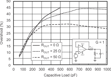
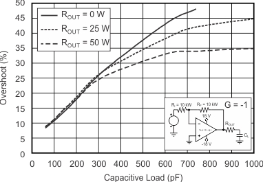
The dynamic characteristics of the OPAx171-Q1 family of devices have been optimized for commonly encountered operating conditions. The combination of low closed-loop gain and high capacitive loads decreases the phase margin of the amplifier and can lead to gain peaking or oscillations. As a result, heavier capacitive loads must be isolated from the output. The simplest way to achieve this isolation is to add a small resistor (for example, ROUT equal to 50 Ω) in series with the output. Figure 38 and Figure 39 show small-signal overshoot versus capacitive load for several values of ROUT. For details of analysis techniques and application circuits, see Applications Bulletin AB-028, available for download from TI.com.
 Figure 38. Small-Signal Overshoot vs Capacitive Load (100-mV Output Step)
  Figure 39. Small-Signal Overshoot vs Capacitive Load (100-mV Output Step)