JAJSCJ9D October   2016  – June 2019 OPA2325 , OPA325 , OPA4325

PRODUCTION DATA.  

  1. 特長
  2. アプリケーション
    1.     オフセット電圧 対 入力同相電圧
  3. 概要
    1.     OPAx325 を ADC ドライバ・アンプとして使用する例
  4. 改訂履歴
  5. Pin Configuration and Functions
    1.     Pin Functions: OPA325
    2.     Pin Functions: OPA2325
    3.     Pin Functions: OPA4325
  6. Specifications
    1. 6.1 Absolute Maximum Ratings
    2. 6.2 ESD Ratings
    3. 6.3 Recommended Operating Conditions
    4. 6.4 Thermal Information: OPA325
    5. 6.5 Thermal Information: OPA2325
    6. 6.6 Thermal Information: OPA4325
    7. 6.7 Electrical Characteristics: VS = 2.2 V to 5.5 V or ±1.1 V to ±2.75 V
    8. 6.8 Typical Characteristics
  7. Detailed Description
    1. 7.1 Overview
    2. 7.2 Functional Block Diagram
    3. 7.3 Feature Description
      1. 7.3.1 Zero-Crossover Input Stage
      2. 7.3.2 Low Input Offset Voltage
      3. 7.3.3 Input and ESD Protection
    4. 7.4 Device Functional Modes
  8. Application and Implementation
    1. 8.1 Application Information
      1. 8.1.1 Operating Characteristics
      2. 8.1.2 Basic Amplifier Configurations
      3. 8.1.3 Driving an Analog-to-Digital Converter
    2. 8.2 Typical Application
      1. 8.2.1 Design Requirements
      2. 8.2.2 Detailed Design Procedure
      3. 8.2.3 Application Curves
  9. Power Supply Recommendations
  10. 10Layout
    1. 10.1 Layout Guidelines
    2. 10.2 Layout Example
  11. 11デバイスおよびドキュメントのサポート
    1. 11.1 ドキュメントのサポート
      1. 11.1.1 関連資料
    2. 11.2 関連リンク
    3. 11.3 ドキュメントの更新通知を受け取る方法
    4. 11.4 コミュニティ・リソース
    5. 11.5 商標
    6. 11.6 静電気放電に関する注意事項
    7. 11.7 Glossary
  12. 12メカニカル、パッケージ、および注文情報

パッケージ・オプション

メカニカル・データ(パッケージ|ピン)
サーマルパッド・メカニカル・データ
発注情報

Input and ESD Protection

The OPAx325 incorporate internal electrostatic discharge (ESD) protection circuits on all pins. In the case of input and output pins, this protection primarily consists of current-steering diodes connected between the input and power-supply pins. These ESD protection diodes also provide in-circuit, input overdrive protection, as long as the current is limited to 10 mA as stated in the Absolute Maximum Ratings table. Figure 43 shows how a series input resistor can be added to the driven input to limit the input current. The added resistor contributes thermal noise at the amplifier input; thus, keep the value to a minimum in noise-sensitive applications.
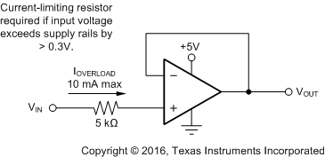
OPA325 OPA2325 OPA4325 Input_Current_Limit_OPA388_SBOS777.gifFigure 43. Input Current Protection