SBOS100B July 1999 – January 2016 OPA551 , OPA552
PRODUCTION DATA.
- 1 Features
- 2 Applications
- 3 Description
- 4 Revision History
- 5 Pin Configuration and Functions
- 6 Specifications
- 7 Detailed Description
- 8 Application and Implementation
- 9 Power Supply Recommendations
- 10Layout
- 11Device and Documentation Support
- 12Mechanical, Packaging, and Orderable Information
パッケージ・オプション
メカニカル・データ(パッケージ|ピン)
サーマルパッド・メカニカル・データ
発注情報
7 Detailed Description
7.1 Overview
The OPA55x devices are low-cost, laser-trimmed, operational amplifiers that feature outstanding low-level accuracy coupled with high output swing. High device performance is maintained as these amplifiers swing to the specified device limits in a wide range of applications. The OPA551 is unity-gain stable while the OPA552 is optimized for gains of 5 or greater.
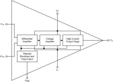
7.2 Functional Block Diagram

7.3 Feature Description
Thermal Shutdown
Internal thermal shutdown circuitry shuts down the output when the die temperature reaches approximately 160°C and resets when the die has cooled to 140°C. The flag pin can be monitored to determine if shutdown has occurred. During normal operation, the current source from the flag pin is less than 50 nA. During shutdown, the flag pin sources 120 µA (typical).
7.3.1 Current Limit
The OPA55x devices are designed with internal current-limiting circuitry that limits the output current to approximately 380 mA. The current limit varies with increasing junction temperature as shown in (Figure 11). This feature, in combination with the thermal protection circuitry, provides protection from many types of overload conditions, including short-circuit to ground.
7.3.2 Input Protection
The OPA55x features internal clamp diodes to protect the inputs when voltages beyond the supply rails are encountered. However, input current must be limited to 5 mA. In some cases, an external series resistor may be required. Many input signals are inherently current-limited; therefore, a limiting resistor may not be required. Consider that a large series resistor, in conjunction with the input capacitance, can affect stability.
7.3.3 Thermal Protection
The OPA55x has thermal shutdown circuitry that protects the amplifier from damage caused by overload conditions. The thermal protection circuitry disables the output when the junction temperature reaches approximately 160°C, allowing the device to cool. When the junction temperature cools to approximately 140°C, the output circuitry is automatically re-enabled.
The thermal shutdown function is not intended to replace proper heat sinking. Activation of the thermal shutdown circuitry is an indication of excessive power dissipation or an inadequate heat sink. Continuously running the amplifier into thermal shutdown can degrade reliability.
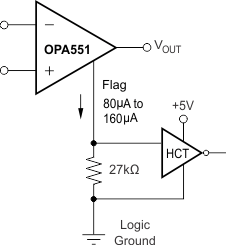
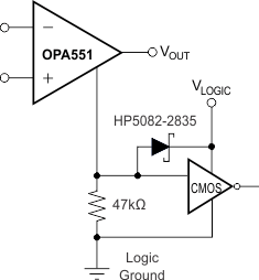
The thermal shutdown indicator (flag) pin can be monitored to determine if shutdown is occurring. During normal operation, the current output from the flag pin is typically 50 nA. During shutdown, the current output from the flag pin increases to 120 μA (typical). This current output allows for easy interfacing to external logic. Refer to Figure 25 and Figure 26 for two examples that implement this function.


7.4 Device Functional Modes
The OPA551 and OPA552 have a single functional mode. The device is operational when the power supply is above 8 V and the junction temperature is below 160°C.