SBOS165B September 2000 – April 2024 OPA627 , OPA637
PRODMIX
- 1
- 1 Features
- 2 Applications
- 3 Description
- 4 Pin Configuration and Functions
-
5 Specifications
- 5.1 Absolute Maximum Ratings
- 5.2 ESD Ratings
- 5.3 Recommended Operating Conditions
- 5.4 Thermal Information: OPA627
- 5.5 Thermal Information: OPA637
- 5.6 Electrical Characteristics: OPA627BU, OPA627AU
- 5.7 Electrical Characteristics: OPA627AM, OPA627BM, OPA627SM
- 5.8 Electrical Characteristics: OPA637
- 5.9 Typical Characteristics
- 6 Detailed Description
- 7 Application and Implementation
- 8 Device and Documentation Support
- 9 Revision History
- 10Mechanical, Packaging, and Orderable Information
パッケージ・オプション
デバイスごとのパッケージ図は、PDF版データシートをご参照ください。
メカニカル・データ(パッケージ|ピン)
- D|8
- LMC|8
サーマルパッド・メカニカル・データ
発注情報
6.3.3 Input Bias Current
The OPA6x7 provide low input bias current. Because the gate current of a FET doubles approximately every 10°C, to achieve lowest input bias current, keep the die temperature as low as possible. The high speed, and therefore higher quiescent current, of the OPA6x7 can lead to higher chip temperature. Proper layout techniques help dissipate heat and reduce chip temperature, thereby lowering IB.
A simple press-on heat sink such as the Burr-Brown model 807HS (TO-99 metal package) can reduce chip temperature by approximately 15°C, lowering the IB to one-third of the warmed-up value. The 807HS heat sink can also reduce low-frequency voltage noise caused by air currents and thermoelectric effects.
Temperature rise in the SOIC packages can be minimized by soldering the device to the circuit board. Wide copper traces also help dissipate heat.
The OPA6x7 can also operate at reduced power supply voltage, to minimize power dissipation and temperature rise. Using ±5V power supplies reduces power dissipation to one-third of that at ±15V.
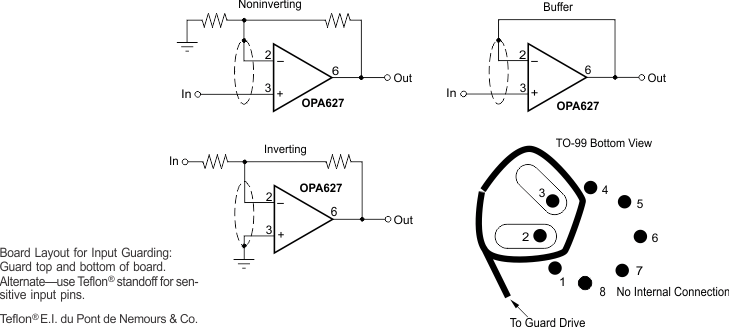
Leakage currents between printed circuit board (PCB) traces can easily exceed the input bias current of the OPA6x7. A circuit board guard pattern reduces leakage effects. By surrounding critical high impedance input circuitry with a low impedance circuit connection at the same potential, leakage current can flow harmlessly to the low-impedance node (see Figure 6-4). The case (TO-99 metal package only) is internally connected to –VS.
Input bias current can also be degraded by improper handling or cleaning. Contamination from handling parts and circuit boards can be removed with cleaning solvents and deionized water. Follow each rinsing operation by a 30-minute bake at 85°C.
Many FET input operational amplifiers exhibit large changes in input bias current with changes in input voltage. Input stage cascode circuitry makes the input bias current of the OPA6x7 virtually constant with wide common-mode voltage changes. The OPA6x7 are a great choice for accurate, high input-impedance buffer applications.
 Figure 6-4 Connection of Input Guard for Lowest IB