SBOS940A May 2019 – March 2020 OPA818
PRODUCTION DATA.
- 1 Features
- 2 Applications
- 3 Description
- 4 Revision History
- 5 Device Comparison Table
- 6 Pin Configuration and Functions
- 7 Specifications
- 8 Detailed Description
- 9 Application and Implementation
- 10Power Supply Recommendations
- 11Layout
- 12Device and Documentation Support
- 13Mechanical, Packaging, and Orderable Information
パッケージ・オプション
メカニカル・データ(パッケージ|ピン)
- DRG|8
サーマルパッド・メカニカル・データ
- DRG|8
発注情報
9.2.2 Non-Inverting Gain of 2 V/V
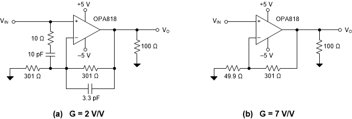
The OPA818 is normally stable in noise gain configurations of greater than 7 V/V when conventional feedback networks are used. The OPA818 can be configured in noise gains of less than 7 V/V by using capacitors in the feedback path and between the inputs to maintain the desired gain at lower frequencies and increase the noise gain at higher frequencies such that the amplifier is stable. Configuration (a) in Figure 55 shows OPA818 configured in a gain of 2 V/V by using capacitors and resistors to shape the noise gain and achieve a phase margin of approximately 51° that is very close to the phase margin achieved for the conventional 7 V/V configuration (b) in Figure 55.
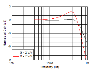
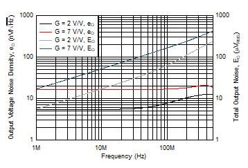
The key benefit of using a decompensated amplifier such as the OPA818 below the minimum stable gain allows taking advantage of the low noise and low distortion performance at powers lower than comparable unity-gain stable architectures. The small-signal frequency response in Figure 55 shows flat AC performance beyond 100 MHz for gain of 2 V/V configuration (a) in Figure 57, and by being in a lower gain configuration versus the minimum stable gain configuration of 7 V/V, the output-referred total noise is also lower (64 nV/√Hz at 100 MHz) as shown in Figure 57 compared to that at 166 nV/√Hz of configuration (b). By reducing the 10-pF input capacitor, higher closed-loop bandwidth can be achieved at the expense of increased peaking and reduced phase margin. Low-capacitance layout by minimizing trace lengths and removing planes under the traces and components connected to the inverting input is critical to minimize parasitic capacitance (see Layout Guidelines). As small as 1 to 2 pF of parasitic capacitance on inverting input will require tweaking the noise-shaping component values to get flat frequency response and the desired phase margin. Configurations in Figure 55 does not take into account this parasitic capacitance but it must be considered for practical purposes. A 45° phase margin is generally acceptable but anything below 40° is not recommended to allow for component, PCB, and process tolerances. Details on the benefits of decompensated architectures are discussed in Using a decompensated op amp for improved performance.
 Figure 55. Non-Inverting Gain of 2 V/V and 7 V/V Configurations
