SLES177B April 2006 – August 2015 PCM1808
PRODUCTION DATA.
- 1 Features
- 2 Applications
- 3 Description
- 4 Revision History
- 5 Pin Configuration and Functions
- 6 Specifications
- 7 Detailed Description
- 8 Application and Implementation
- 9 Power Supply Recommendations
- 10Layout
- 11Device and Documentation Support
- 12Mechanical, Packaging, and Orderable Information
パッケージ・オプション
メカニカル・データ(パッケージ|ピン)
- PW|14
サーマルパッド・メカニカル・データ
- PW|14
発注情報
7 Detailed Description
7.1 Overview
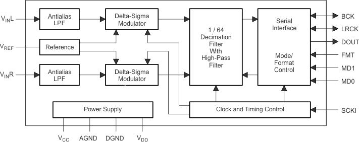
The PCM1808 is high-performance, low-cost, single-chip, stereo analog-to-digital converter with single-ended analog voltage input. The PCM1808 uses a delta-sigma modulator with 64-times oversampling and includes a digital decimation filter and high-pass filter that removes the dc component of the input signal. For various applications, the PCM1808 supports master and slave mode and two data formats in serial audio interface up to 96-kHz sampling. These features are controlled through hardware by pulling pins high or low with resistors or a controller GPIO. The PCM1808 also supports a power-down and reset function by means of halting the system clock.
7.2 Functional Block Diagram

7.3 Feature Description
7.3.1 Hardware Control
Pins FMT, MD0, and MD1 allow the device to be controlled by either pullup or pulldown resistors as well as GPIO from a digital IC. These controls allow the option of switching between I2S or left-justified, and in which interface mode the device operates.
7.3.2 System Clock
The PCM1808 device supports 256 fS, 384 fS, and 512 fS as system clock, where fS is the audio sampling frequency. The system clock input must be on SCKI (pin 6).
The PCM1808 device has a system-clock detection circuit which automatically senses if the system-clock operation is at 256 fS, 384 fS, or 512 fS in slave mode. In master mode, control of the system clock frequency must be through the serial control port, which uses MD1 (pin 11) and MD0 (pin 10). An internal circuit automatically divides down the system clock to generate frequencies of 128 fS and 64 fS, which operate the digital filter and the delta-sigma modulator, respectively.
Table 1 shows some typical relationships between sampling frequency and system clock frequency, and Figure 1 shows system clock timing.
Table 1. Sampling Frequency and System Clock Frequency
| SAMPLING FREQUENCY (kHz) | SYSTEM CLOCK FREQUENCY (fSCLK) (MHz) | ||
|---|---|---|---|
| 256 fS | 384 fS | 512 fS | |
| 8 | 2.048 | 3.072 | 4.096 |
| 16 | 4.096 | 6.144 | 8.192 |
| 32 | 8.192 | 12.288 | 16.384 |
| 44.1 | 11.2896 | 16.9344 | 22.5792 |
| 48 | 12.288 | 18.432 | 24.576 |
| 64 | 16.384 | 24.576 | 32.768 |
| 88.2 | 22.5792 | 33.8688 | 45.1584 |
| 96 | 24.576 | 36.864 | 49.152 |
7.3.3 Synchronization With Digital Audio System
In slave mode, the PCM1808 device operates under LRCK (pin 7), synchronized with system clock SCKI (pin 6). The PCM1808 device does not require a specific phase relationship between LRCK and SCKI, but does require the synchronization of LRCK and SCKI.
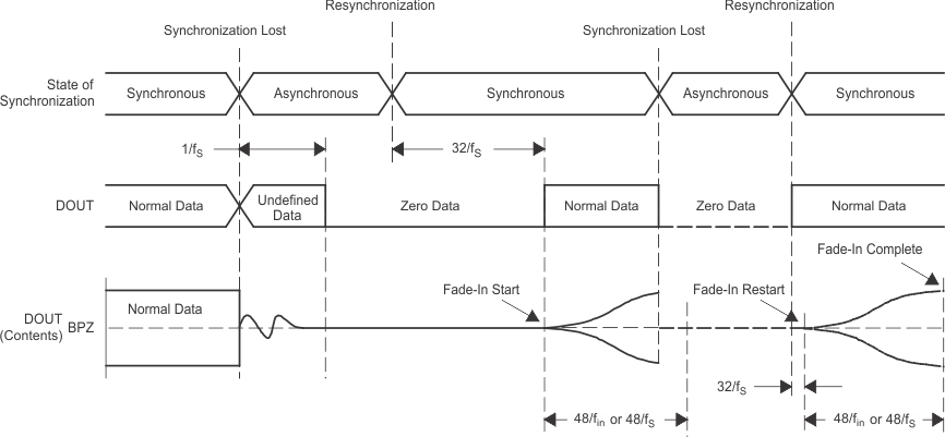
If the relationship between LRCK and SCKI changes more than ±6 BCKs for 64 BCK/frame (±5 BCKs for 48 BCK/frame) during one sample period due to LRCK or SCKI jitter, internal operation of the ADC halts within 1 / fS and digital output goes to zero data (BPZ code) until resynchronization between LRCK and SCKI occurs.
In the case of changes less than ±5 BCKs for 64 BCK/frame (±4 BCKs for 48 BCK/frame), resynchronization does not occur, and the previously described digital output control and discontinuity do not occur.
Figure 23 illustrates the digital output response for loss of synchronization and resynchronization. During undefined data, the PCM1808 device can generate some noise in the audio signal. Also, the transition of normal data to undefined data creates a discontinuity in the digital output data, which can generate some noise in the audio signal. The digital output is valid after resynchronization completes and the time of 32 / fS has elapsed. Because the fade-in operation is performed, it takes additional time of 48 / fin or 48 / fS to obtain the level corresponding to the analog input signal. In the case of loss of synchronization during the fade-in or fade-out operation, the operation stops and DOUT (pin 9) goes to zero data immediately. The fade-in operation resumes from mute after the time of 32 / fS following resynchronization.
 Figure 23. ADC Digital Output for Loss of Synchronization and Resynchronization
7.3.4 Power On
The PCM1808 device has an internal power-on-reset circuit, and initialization (reset) occurs automatically when the power supply (VDD) exceeds 2.2 V (typical). While VDD < 2.2 V (typical), and for 1024 system-clock counts after VDD > 2.2 V (typical), the PCM1808 device stays in the reset state and the digital output remains zero. After release of the reset state, 8960 / fS seconds must pass before the digital output becomes valid. Because of the performing of the fade-in operation, it takes additional time of 48 / fin or 48 / fS to obtain the data corresponding to the analog input signal. Figure 2 illustrates the power-on timing and the digital output.
7.3.5 Serial Audio Data Interface
The PCM1808 device interfaces the audio system through LRCK (pin 7), BCK (pin 8), and DOUT (pin 9).
7.3.5.1 Interface Mode
MD1 (pin 11) and MD0 (pin 10) select master mode and slave mode as interface modes, both of which the PCM1808 device supports.Table 2 shows the interface-mode selections. It is necessary to set MD1 and MD0 prior to power on.
In master mode, the PCM1808 device provides the timing of serial audio data communications between the PCM1808 device and the digital audio processor or external circuit. While in slave mode, the PCM1808 device receives the timing for data transfer from an external controller.
Table 2. Interface Modes
| MD1 (PIN 11) | MD0 (PIN 10) | INTERFACE MODE |
|---|---|---|
| Low | Low | Slave mode (256 fS, 384 fS, 512 fS autodetection) |
| Low | High | Master mode (512 fS) |
| High | Low | Master mode (384 fS) |
| High | High | Master mode (256 fS) |
7.3.5.1.1 Master Mode
In master mode, BCK and LRCK work as output pins, timing which from the clock circuit of the PCM1808 device controls these pins. The frequency of BCK is constant at 64 BCK/frame.
7.3.5.1.2 Slave Mode
In slave mode, BCK and LRCK work as input pins. The PCM1808 device accepts 64-BCK/frame or 48-BCK/frame format (only for a 384-fS system clock), not 32-BCK/frame format.
7.3.5.2 Data Format
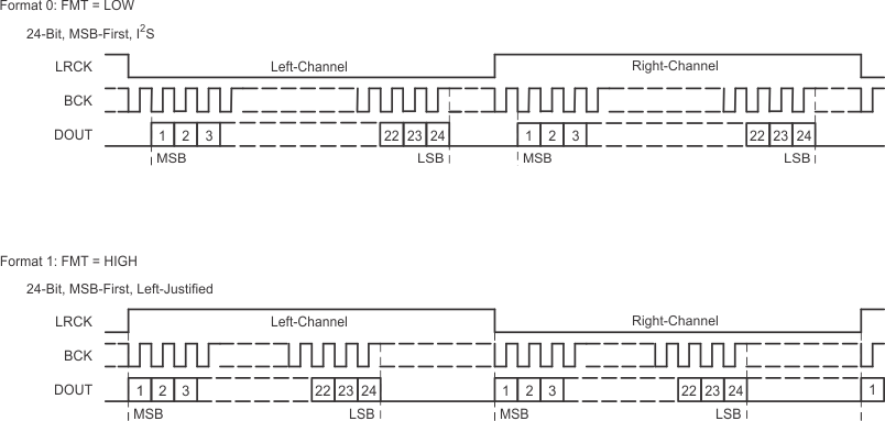
Table 3. Data Format
| FORMAT NO. | FMT (Pin 12) | FORMAT |
|---|---|---|
| 0 | Low | I2S, 24-bit |
| 1 | High | Left-justified, 24-bit |
 Figure 24. Audio Data Format (LRCK and BCK Work as Inputs in Slave Mode
 and as Outputs in Master Mode)
7.4 Device Functional Modes
7.4.1 Fade-In and Fade-Out Functions
The PCM1808 device has fade-in and fade-out functions on DOUT (pin 9) to avoid pop noise, and the functions come into operation in some cases as described in several following sections. Performance of the level changes from 0 dB to mute or mute to 0 dB employs calculated pseudo S-shaped characteristics with zero-cross detection. Because of the zero-cross detection, the time needed for the fade-in and fade-out depends on the analog input frequency (fin). It takes 48 / fin to complete the processing. If there is no zero-cross during 8192 / fS, a forced DOUT fade-in or fade-out occurs during 48 / fS (TIME OUT). Figure 25 illustrates the fade-in and fade-out operation processing.
 Figure 25. Fade-In and Fade-Out Operations
7.4.2 Clock-Halt Power-Down and Reset Function
The PCM1808 device has a power-down and reset function. Halting SCKI (pin 6) in both master and slave modes triggers this function. The function is available any time after power on. Reset and power down occur automatically 4 μs (minimum) after the halt of SCKI. During assertion of the clock-halt reset, the PCM1808 device stays in the reset and power-down mode, with DOUT (pin 9) forced to zero. Release the reset and power-down mode requires the supply of SCKI. The digital output is valid after release of the reset state and elapse of the time of 1024 SCKI + 8960 / fS. Performing the fade-in operation takes additional time of 48 / fin or 48 / fS to attain the level corresponding to the analog input signal. Figure 3 illustrates the clock-halt reset timing.
To avoid ADC performance degradation, BCK (pin 8) and LRCK (pin 7) must synchronize with SCKI within 4480 / fS after the resumption of SCKI. If it takes more than 4480 / fS for BCK and LRCK to synchronize with SCKI, mask SCKI until it again achieves synchronization, taking care of glitch and jitter. See the typical circuit connection diagram, Figure 26.
To avoid ADC performance degradation, assertion of the clock-halt reset is necessary when changing system clock SCKI or the audio interface clocks BCK and LRCK (sampling rate fS) on the fly.