SBOS207C October   2001  – December 2015 PGA2310

PRODUCTION DATA.  

  1. Features
  2. Applications
  3. Description
  4. Revision History
  5. Pin Configuration and Functions
  6. Specifications
    1. 6.1 Absolute Maximum Ratings
    2. 6.2 ESD Ratings
    3. 6.3 Recommended Operating Conditions
    4. 6.4 Thermal Information
    5. 6.5 Electrical Characteristics
    6. 6.6 Typical Characteristics
  7. Detailed Description
    1. 7.1 Overview
    2. 7.2 Functional Block Diagram
    3. 7.3 Feature Description
      1. 7.3.1 Analog Inputs and Outputs
      2. 7.3.2 Serial Control Port
      3. 7.3.3 Gain Settings
      4. 7.3.4 Daisy-Chaining Multiple PGA2310 Devices
      5. 7.3.5 Zero Crossing Detection
      6. 7.3.6 Mute Function
    4. 7.4 Device Functional Modes
      1. 7.4.1 Power-Up State
  8. Application and Implementation
    1. 8.1 Application Information
    2. 8.2 Typical Application
      1. 8.2.1 Design Requirements
      2. 8.2.2 Detailed Design Procedure
      3. 8.2.3 Application Curve
  9. Power Supply Recommendations
  10. 10Layout
    1. 10.1 Layout Guidelines
    2. 10.2 Layout Example
  11. 11Device and Documentation Support
    1. 11.1 Device Support
      1. 11.1.1 Development Support
    2. 11.2 Documentation Support
      1. 11.2.1 Related Documentation
    3. 11.3 Community Resources
    4. 11.4 Trademarks
    5. 11.5 Electrostatic Discharge Caution
    6. 11.6 Glossary
  12. 12Mechanical, Packaging, and Orderable Information

パッケージ・オプション

メカニカル・データ(パッケージ|ピン)
サーマルパッド・メカニカル・データ
発注情報

10 Layout

10.1 Layout Guidelines

TI recommends that the ground planes for the digital and analog sections of the printed-circuit-board (PCB) be separate from one another. The planes should be connected at a single point. Figure 15 shows the recommended PCB floor plan for the PGA2310.

The PGA2310 is mounted so that it straddles the split between the digital and analog ground planes. Pins 1 through 8 are oriented to the digital side of the board, while pins 9 through 16 are on the analog side of the board.

10.2 Layout Example
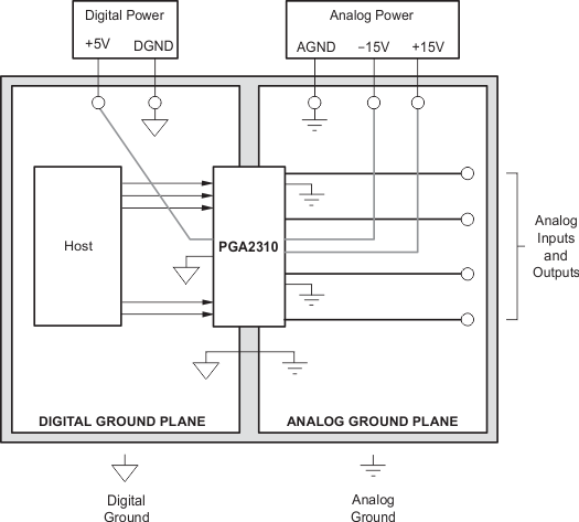
PGA2310 pcb_layout.gif Figure 15. Typical PCB Layout Floor Plan