SLDS185D March 2012 – June 2016 PGA450-Q1
PRODUCTION DATA.
- 1 Features
- 2 Applications
- 3 Description
- 4 Revision History
- 5 Pin Configuration and Functions
-
6 Specifications
- 6.1 Absolute Maximum Ratings
- 6.2 ESD Ratings: AEC Q100
- 6.3 ESD Ratings: IEC61000-4-2
- 6.4 Recommended Operating Conditions
- 6.5 Thermal Information
- 6.6 Electrical Characteristics
- 6.7 Electrical Characteristics — LIN 2.1 Slave and Buffered SCI
- 6.8 Electrical Characteristics — SPI Interface
- 6.9 Timing Requirements
- 6.10 Timing Requirements — LIN 2.1 Slave and Buffered SCI
- 6.11 Timing Requirements — SPI Interface
- 6.12 Switching Characteristics
- 6.13 Digital Datapath Filter Switching Characteristics
- 6.14 Typical Characteristics
-
7 Detailed Description
- 7.1 Overview
- 7.2 Functional Block Diagram
- 7.3
Feature Description
- 7.3.1 Power Supply Block
- 7.3.2 VREG
- 7.3.3 Clock
- 7.3.4 Low-Side Drive FETs
- 7.3.5 Burst Generator
- 7.3.6 Low-Noise Amplifier
- 7.3.7 Analog-to-Digital Converter
- 7.3.8 Digital Data Path
- 7.3.9 Transducer Saturation Time
- 7.3.10 Temperature Sensor
- 7.3.11 Free-Running Timer
- 7.3.12 GPIOs
- 7.3.13 8051W UART
- 7.3.14 8051 WARP Core
- 7.3.15 Memory
- 7.3.16
LIN 2.1 Slave and Buffered SCI
- 7.3.16.1 Physical Layer
- 7.3.16.2 LIN Slave Mode
- 7.3.16.3 SCI Buffered Mode
- 7.3.16.4 Connection of LIN Pin to 8051W
- 7.4 Device Functional Modes
- 7.5
Programming
- 7.5.1 SPI Interface
- 7.5.2 Diagnostics
- 7.5.3 8051W Interrupts
- 7.5.4 Instructions
- 7.5.5 8051W Port Usage
- 7.6
Register Maps
- 7.6.1
SFR Registers
- 7.6.1.1 I/O Ports (P0, P1, P2, P3) Registers
- 7.6.1.2 Stack Pointer Register (offset = 0x81) [reset = 0]
- 7.6.1.3 Data Pointer Registers
- 7.6.1.4 Power Control Register (offset = 0x87) [reset = 0]
- 7.6.1.5 Timer and Counter Control Register (offset = 0x88) [reset = 0]
- 7.6.1.6 Timer and Counter Mode Register (offset = 0x89) [reset = 0]
- 7.6.1.7 Timer and Counter Data Registers (TL0, TL1, TH0, TH1)
- 7.6.1.8 UART Control Register (offset = 0x98) [reset = 0]
- 7.6.1.9 UART Data Register (offset = 0x99) [reset = 0]
- 7.6.1.10 Interrupt Enable Register 0 (offset = 0xA8) [reset = 0]
- 7.6.1.11 Interrupt Enable Register 1 (offset = 0xE8) [reset = 0]
- 7.6.1.12 Interrupt Priority Register 0 (offset = 0xB8) [reset = 0]
- 7.6.1.13 Interrupt Priority Register 1 (offset = 0xF8) [reset = 0]
- 7.6.1.14 Program Status Word Register (offset = 0xD0) [reset = 0]
- 7.6.1.15 Accumulator Register (offset = 0xE0) [reset = 0]
- 7.6.1.16 B Register (offset = 0xF0) [reset = 0]
- 7.6.2
ESFR Registers
- 7.6.2.1 Bandpass Filter Coefficient B1 (BPF_B1) Register
- 7.6.2.2 Bandpass Filter Coefficient A2 (BPF_A2) Registers
- 7.6.2.3 Band-Pass Filter Coefficient A3 (BPF_A3) Register
- 7.6.2.4 Low-Pass Filter Coefficient B1 (LPF_B1) Registers
- 7.6.2.5 Low-Pass Filter Coefficient A2 (LPF_A2) Registers
- 7.6.2.6 Downsample Register (offset = 0xA5) [reset = 0]
- 7.6.2.7 BURST ON A Duration (ON_A) Registers
- 7.6.2.8 BURST OFFA Duration (OFF_A) Register
- 7.6.2.9 BURST ON B Duration (ON_B) Registers
- 7.6.2.10 BURST OFF B Duration (OFF_B) Register
- 7.6.2.11 Pulse Count A Register (offset = 0xAF) [reset = 0]
- 7.6.2.12 Pulse Count B Register (offset = 0xB1) [reset = 0]
- 7.6.2.13 Deadtime Register (offset = 0xB2) [reset = 0]
- 7.6.2.14 Burst Mode Register (offset = 0xB3) [reset = 0]
- 7.6.2.15 Temperature Sensor Register (offset = 0xB4) [reset = 0]
- 7.6.2.16 Saturation Deglitch Time Register (offset = 0xB5) [reset = 0]
- 7.6.2.17 Saturation Time Capture Register (offset = 0xB6) [reset = 0]
- 7.6.2.18 Control 1 Register (offset = 0xB7) [reset = 0]
- 7.6.2.19 Blanking Timer Register (offset = 0xB9) [reset = 0]
- 7.6.2.20 Free Running Timer (FRT) Registers
- 7.6.2.21 GPIO Control Register (offset = 0xBC) [reset = 0]
- 7.6.2.22 Clock Select Register (offset = 0xBD) [reset = 0]
- 7.6.2.23 Watchdog Enable Register (offset = 0xBE) [reset = 0]
- 7.6.2.24 LIN/SCI Select Register (offset = 0xBF) [reset = 0]
- 7.6.2.25 EEPROM Control Register (offset = 0xC0) [reset = 0]
- 7.6.2.26 Status 1 (STATUS1) Register (offset = 0xC1) [reset = 0]
- 7.6.2.27 Status 2 Register (offset = 0xC2) [reset = 0]
- 7.6.2.28 Power Mode Register (offset = 0xC3) [reset = 0]
- 7.6.2.29 Datapath and SCI Control Register (offset = 0xC4) [reset = 0]
- 7.6.2.30 FIFO Control Register (offset = 0xC5) [reset = ]
- 7.6.2.31 Enable Control Register (offset = 0xC8) [reset = 0]
- 7.6.2.32 LIN/SCI Rx Data (RX_DATAx) Register (offset = 0xC9 to 0xD1) [reset = 0]
- 7.6.2.33 LIN PID Register (offset = 0xD2) [reset = 0]
- 7.6.2.34 LIN/SCI Tx Data Registers (offset = 0xD3 to 0xDA) [reset = 0]
- 7.6.2.35 LIN/SCI Data Count Register (offset = 0xDB) [reset = 0]
- 7.6.2.36 LIN Configuration Register (offset = 0xDC) [reset = 0x40]
- 7.6.2.37 LIN Control Register (offset = 0xDD) [reset = 0]
- 7.6.2.38 LIN STATUS Register (offset = 0xDE) [reset = 0]
- 7.6.2.39 FIFO Pointer (FIFO_POINTER) Registers
- 7.6.2.40 VREG Select Register (offset = 0xE2) [reset = 0]
- 7.6.2.41 Sync Count (SYNC_COUNT) Registers
- 7.6.2.42 TEMP/DAC Control Register (offset = 0xE5) [reset = 0]
- 7.6.2.43 Oscillator Sync Control Register (offset = 0xE6) [reset = 0]
- 7.6.3 TEST Registers
- 7.6.1
SFR Registers
- 8 Application and Implementation
- 9 Power Supply Recommendations
- 10Layout
- 11Device and Documentation Support
- 12Mechanical, Packaging, and Orderable Information
8 Application and Implementation
NOTE
Information in the following applications sections is not part of the TI component specification, and TI does not warrant its accuracy or completeness. TI’s customers are responsible for determining suitability of components for their purposes. Customers should validate and test their design implementation to confirm system functionality.
8.1 Application Information
The PGA450-Q1 must be paired with an external transducer. The PGA450-Q1 drives the transducer and then filters and processes the returned echo signal sensed by the transducer. The transducer should be chosen based on the resonant frequency, input voltage requirements, sensitivity, beam pattern, and decay time. The PGA450-Q1 meets most transducer requirements by adjusting the driving frequency, driving voltage, and bandpass center frequency. The external transformer should be chosen to meet the input voltage requirements of the transducer and to have a high-enough saturation current.
The interface options include LIN, SCI, UART, and SPI. The SPI must be used when programming the memory of the PGA450-Q1, but after that any of the other interfaces can be used for communication. After a distance measurement is initiated, the PGA450-Q1 can return the measured distance through a communication interface.
8.2 Typical Application
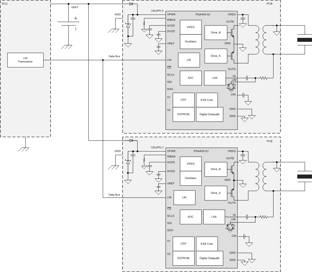
In the typical application, the PGA450-Q1 is paired with one transducer which are located on one PCB as one sense node. Each PCB uses a three-wire interface, power, ground, and LIN. Multiple PCBs can be connected in parallel as shown in Figure 127. If a different communication method is used, then more wires may be needed.
 Figure 127. Typical Application Schematic
8.2.1 Design Parameters
For this design example, use the following parameters:
- ftransducer = 58 kHz
- VPWR = 12 V
- dmin = 15 cm
- dmax = 5 m
8.2.2 Detailed Design Procedure
8.2.2.1 Hardware
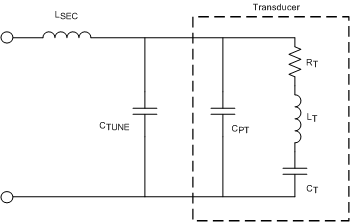
The hardware design for the PGA450 consists of selecting a transducer and supporting passive components. When a transducer is selected, the next step in the design process is to select a transformer based on the characteristics of the transducer. Figure 128 shows the electrical model of the transducer. The secondary winding of the transformer should be selected to match the resonant frequency of the transducer. A tuning capacitor can be used to assist with this requirement.
 Figure 128. Transducer and Transformer Electrical Model

The low-side drivers force a voltage across the transducers equal to the VREG voltage. Either low-side driver can be used with a single-ended transformer or a center-tapped transformer can be used with both low-side drivers for push-pull mode. Single-ended mode causes the voltage on the secondary side of the windings to be approximately the turn ratio multiplied by the VREG voltage. Push-pull mode doubles the voltage. Select the transformer, the value of VREG, and circuit configuration based on the VPP value of the transducer. Also consider that as current is pulled from the VREG capacitor, the voltage at the VREG pin will droop. Finally, ensure that the transformer saturation current is sufficient.
8.2.2.2 Firmware
The PGA450-Q1 must be programmed to work with the selected transducer and can be optimized for the desired range. For this example, two different firmware settings will be used: one to optimize short-distance detection and one to optimize long-distance detection. Program the registers listed in Table 117 to program the device to work with the selected transducer.
Table 117. Registers to Tune for Optimization
| SHORT DISTANCE OPTIMIZATION | LONG DISTANCE OPTIMIZATION | |
|---|---|---|
| Bandpass filter | BPF_B1_MSB = 0x03 | |
| BPF_B1_LSB = 0x2D | ||
| BPF_A2_MSB = 0xEC | ||
| BPF_A2_LSB = 0x3D | ||
| BPF_A3_MSB = 0xF9 | ||
| BPF_A3_LSB = 0xA5 | ||
| Downsample rate | DOWNSAMPLE = 0x28 | |
| Low-pass filter | LPF_B1_MSB = 0x2D | |
| LPF_B1_LSB = 0x68 | ||
| LPF_A2_MSB = 0x25 | ||
| LPF_A2_LSB = 0x30 | ||
| Low-side drivers | BURST_ONA_MSB = 0x00 | |
| BURST_ONA_LSB = 0x8A | ||
| BURST_OFFA_MSB = 0x00 | ||
| BURST_OFFA_LSB = 0x8A | ||
| BURST_ONB_MSB = 0x00 | ||
| BURST_ONB_LSB = 0x8A | ||
| BURST_OFFB_MSB = 0x00 | ||
| BURST_OFFB_LSB = 0x8A | ||
| Pulse count | PULSE_CNTA = 0x01 | PULSE_CNTA = 0x12 |
| Blanking timer | BLANKING_TIMER = 0x27 | BLANKING_TIMER = 0xFF |
| FIFO mode | FIFO_CTRL = 0x07 | FIFO_CTRL = 0x06 |
8.2.2.2.1 Band-pass Filter Coefficients
The bandpass filter coefficients are selected by referring to Table 6 and Table 7. A bandwidth of 4 kHz was selected for this example. A wider bandwidth can be used if the transducer center frequency has more variation or for applications that must pick up possible frequency shifts caused by movement or environmental conditions. A wider bandwidth corresponds to more noise, therefore, the smallest bandwidth that fits the application should be selected.
- BPF_B1_MSB = 0x03
- BPF_B1_LSB = 0x2D
- BPF_A2_MSB = 0xEC
- BPF_A2_LSB = 0x3D
- BPF_A3_MSB = 0xF9
- BPF_A3_LSB = 0xA5
8.2.2.2.2 Downsample Rate
With only 768 bytes available in the FIFO RAM, the downsample rate allows some flexibility for selecting how often samples are stored. A smaller downsample rate provides more resolution but the maximum distance stored will be shorter.

where
- dmax = maximum distance detection required of application.
- fs = ADC sampling frequency, 1 MHz.
- FIFO = FIFO RAM memory size, 768.
- vsound = speed of sound, through air at room temp = 343 m/s.

To add some margin, a downsampling rate of 40 was selected for this example, which is 0x28 in hexadecimal.
DOWNSAMPLE = 0x28
8.2.2.2.3 Low-Pass Filter Coefficients
The low-pass filter coefficients are selected by referring to Table 8. For this example, a cutoff frequency of 4 kHz is used. A smaller cutoff frequency can be used to further zoom in around the center frequency of the transducer; however, ensure to consider the transducer frequency variation across process and temperature.
- LPF_B1_MSB = 0x2D
- LPF_B1_LSB = 0x68
- LPF_A2_MSB = 0x25
- LPF_A2_LSB = 0x30
8.2.2.2.4 Pulse Count
Th pulse count sets the number of pulses driven by the low-side drivers per measurement burst. To optimize the minimum measurable distance, a small number of pulses should be used. To detect distances farther away, more pulses should be sent to maximize the sent signal strength.
- Short distance mode, 1 pulse:
- PULSE_CNTA = 0x01
- Long distance mode, 16 pulses:
- PULSE_CNTA = 0x12
8.2.2.2.5 Blanking Timer
The blanking timer setting allows the user to delay when the FIFO RAM begins storing samples. Immediately after the transducer is excited, the signal is too large to extract useful information from. To maximize the efficiency of the data stored in the FIFO, the blanking timer can be used so that this initial saturated section of data is not stored. For this example, the blanking time was selected by first examining the resulting waveform when the blanking time was 0. From this, the saturated region can be observed. Set the blanking timer to remove most of this saturated region.
- Short distance mode, set to remove the saturated echo region from the echo data:
- BLANKING_TIMER = 0x27
- Long distance mode, maximize blanking timer to increase maximum distance:
- BLANKING_TIMER = 0xFF
8.2.2.2.6 FIFO Mode
The digital datapath of the PGA450-Q1 is 12 bits; however, storing all 12 bits quickly uses up more of the 768 bytes of FIFO RAM which reduces the range of distances that can be measured. An alternative is to store only 8 bits in the FIFO RAM. Storing the lower 8 bits maximizes the resolution and is helpful for measuring long distances. For measuring short distances, minimizing the saturation time is important, therefore, the middle 8 bits can be used.
- Short distance mode, middle 8 bits are stored [10:3]
- FIFO_CTRL = 0x07
- Long distance mode, lower 8 bits are stored:
- FIFO_CTRL = 0x06
8.2.2.3 OUT_A and OUT_B On and Off Times
These on and off times dictate the driving frequency of the low-side drivers. Typically these times will match the center frequency of the transducer.

8.2.3 Application Curves
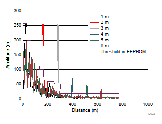
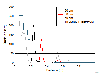
These application curves show the results of using the settings derived above to measure a 1-m tall, 76-mm wide PVC pipe at various distances. Several runs are plotted on top of each other. The y-axis shows the signal strength of the returned signal and the x-axis shows the distance. To determine where the object is located, a threshold can be used to compare the amplitude of the echo data at each FIFO memory location. When the incoming data surpasses the threshold, the PGA450-Q1 can flag that location as the measured distance. This threshold scheme must be programmed into the microcontroller of the PGA450-Q1.
 Figure 129. Long Distance Measurements
 Figure 130. Short Distance Measurements