JAJSFQ5C July 2018 – October 2020 REF34-Q1
PRODUCTION DATA
- 1 特長
- 2 アプリケーション
- 3 概要
- 4 Revision History
- 5 Device Comparison Table
- 6 Pin Configuration and Functions
- 7 Specifications
- 8 Typical Characteristics
- 9 Parameter Measurement Information
- 10Detailed Description
- 11Application and Implementation
- 12Power Supply Recommendations
- 13Layout
- 14Device and Documentation Support
- 15Mechanical, Packaging, and Orderable Information
パッケージ・オプション
メカニカル・データ(パッケージ|ピン)
サーマルパッド・メカニカル・データ
発注情報
9.1 Solder Heat Shift
The materials used in the manufacture of the REF34-Q1 have differing coefficients of thermal expansion, resulting in stress on the device die when the part is heated. Mechanical and thermal stress on the device die can cause the output voltages to shift, degrading the initial accuracy specifications of the product. Reflow soldering is a common cause of this error.
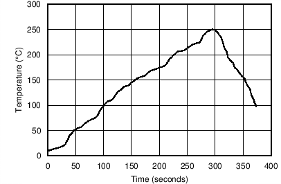
In order to illustrate this effect, a total of 32 devices were soldered on four printed circuit boards [16 devices on each printed circuit board (PCB)] using lead-free solder paste and the paste manufacturer suggested reflow profile. The reflow profile is as shown in Figure 9-1. The printed circuit board is comprised of FR4 material. The board thickness is 1.65 mm and the area is 114 mm × 152 mm. All measurements were taken after baking at 150°C.
 Figure 9-1 Reflow Profile
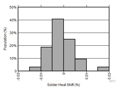
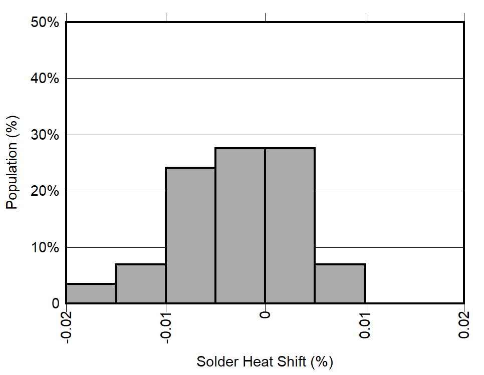
The reference output voltage is measured before and after the reflow process; the typical shift is displayed in Figure 9-2. Although all tested units exhibit very low shifts (< 0.01%), higher shifts are also possible depending on the size, thickness, and material of the printed circuit board. An important note is that the histograms display the typical shift for exposure to a single reflow profile. Exposure to multiple reflows, as is common on PCBs with surface-mount components on both sides, causes additional shifts in the output bias voltage. If the PCB is exposed to multiple reflows, the device must be soldered in the second pass to minimize its exposure to thermal stress.
 Figure 9-2 Solder Heat
Shift Distribution, VREF (%) - DBV Package
 Figure 9-3 Solder Heat
Shift Distribution, VREF (%) - DGK Package