JAJSGI2I september   2015  – august 2023 SN6505A , SN6505B

PRODUCTION DATA  

  1.   1
  2. 特長
  3. アプリケーション
  4. 概要
  5. Revision History
  6. Pin Configuration and Functions
  7. Specifications
    1. 6.1 Absolute Maximum Ratings
    2. 6.2 ESD Ratings
    3. 6.3 Recommended Operating Conditions
    4. 6.4 Thermal Information
    5. 6.5 Electrical Characteristics
    6. 6.6 Timing Requirements
    7. 6.7 Typical Characteristics, SN6505A
    8. 6.8 Typical Characteristics, SN6505B
  8. Parameter Measurement Information
  9. Detailed Description
    1. 8.1 Overview
    2. 8.2 Functional Block Diagram
    3. 8.3 Feature Description
      1. 8.3.1 Push-Pull Converter
      2. 8.3.2 Core Magnetization
    4. 8.4 Device Functional Modes
      1. 8.4.1 Start-Up Mode
        1. 8.4.1.1 Soft-Start
      2. 8.4.2 Operating Mode
      3. 8.4.3 Shutdown-Mode
      4. 8.4.4 Spread Spectrum Clocking
      5. 8.4.5 External Clock Mode
  10. Application and Implementation
    1. 9.1 Application Information
    2. 9.2 Typical Application
      1. 9.2.1 Design Requirements
      2. 9.2.2 Detailed Design Procedure
        1. 9.2.2.1 Drive Capability
        2. 9.2.2.2 LDO Selection
        3. 9.2.2.3 Diode Selection
        4. 9.2.2.4 Capacitor Selection
        5. 9.2.2.5 Transformer Selection
          1. 9.2.2.5.1 V-t Product Calculation
          2. 9.2.2.5.2 Turns Ratio Estimate
          3. 9.2.2.5.3 Recommended Transformers
      3. 9.2.3 Application Curves
      4. 9.2.4 System Examples
        1. 9.2.4.1 Higher Output Voltage Designs
        2. 9.2.4.2 Application Circuits
  11. 10Power Supply Recommendations
  12. 11Layout
    1. 11.1 Layout Guidelines
    2. 11.2 Layout Example
  13. 12Device and Documentation Support
    1. 12.1 Device Support
    2. 12.2 Documentation Support
      1. 12.2.1 Related Documentation
    3. 12.3 Related Links
    4. 12.4 Receiving Notification of Documentation Updates
    5. 12.5 Community Resources
    6. 12.6 Trademarks
  14. 13Mechanical, Packaging, and Orderable Information

パッケージ・オプション

メカニカル・データ(パッケージ|ピン)
サーマルパッド・メカニカル・データ
発注情報

Core Magnetization

Figure 8-2 shows the ideal magnetizing curve for a push-pull converter with B as the magnetic flux density and H as the magnetic field strength. When Q1 conducts the magnetic flux is pushed from A to A’, and when Q2 conducts the flux is pulled back from A’ to A. The difference in flux and thus in flux density is proportional to the product of the primary voltage, VP, and the time, tON, it is applied to the primary: B ≈ VP × tON.
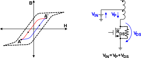
GUID-C58C2E25-E9F3-46EB-B3AF-40CBDE036F3B-low.gifFigure 8-2 Core Magnetization and Self-Regulation Through Positive Temperature Coefficient of RDS(on)

This volt-seconds (V-t) product is important as it determines the core magnetization during each switching cycle. If the V-t products of both phases are not identical, an imbalance in flux density swing results with an offset from the origin of the B-H curve. If balance is not restored, the offset increases with each following cycle and the transformer slowly creeps toward the saturation region.