JAJSMH9O august 2009 – july 2023 SN65HVD3082E , SN65HVD3085E , SN65HVD3088E , SN75HVD3082E
PRODUCTION DATA
- 1
- 1 特長
- 2 アプリケーション
- 3 概要
- 4 Revision History
- 5 Pin Configuration and Functions
-
6 Specifications
- 6.1 Absolute Maximum Ratings
- 6.2 ESD Ratings
- 6.3 Recommended Operating Conditions
- 6.4 Thermal Information, SN65HVD308xE
- 6.5 Thermal Information, SNx5HVD3082E
- 6.6 Electrical Characteristics: Driver
- 6.7 Electrical Characteristics: Receiver
- 6.8 Electrical Characteristics
- 6.9 Switching Characteristics: Driver
- 6.10 Switching Characteristics
- 6.11 Typical Characteristics
- 7 Parameter Measurement Information
- 8 Detailed Description
- 9 Application and Implementation
- 10Power Supply Recommendations
- 11Layout
- 12Device and Documentation Support
- 13Mechanical, Packaging, and Orderable Information
パッケージ・オプション
メカニカル・データ(パッケージ|ピン)
サーマルパッド・メカニカル・データ
発注情報
7 Parameter Measurement Information
Test load capacitance includes probe and jig capacitance (unless otherwise specified). Signal generator characteristics: rise and fall time < 6 ns, pulse rate 100 kHz, 50% duty cycle. ZO = 50 Ω (unless otherwise specified).
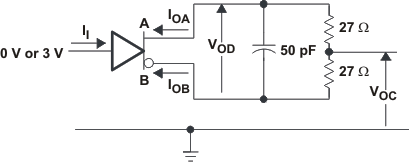 Figure 7-1 Driver
Test Circuit, VOD and VOC Without Common-Mode
Loading
 Figure 7-2 Driver
Test Circuit, VOD With Common-Mode Loading
 Figure 7-3 Driver
VOC Test Circuit and Waveforms
 Figure 7-4 Driver
Switching Test Circuit and Waveforms
 Figure 7-5 Driver
Enable and Disable Test Circuit and Waveforms, High Output
 Figure 7-6 Driver
Enable and Disable Test Circuit and Waveforms, Low Output
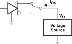 Figure 7-7 Driver
Short-Circuit
 |
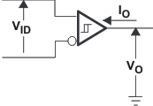 Figure 7-8 Receiver
Switching Test Circuit and Waveforms
 |
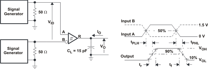 Figure 7-9 Receiver
Switching Test Circuit and Waveforms
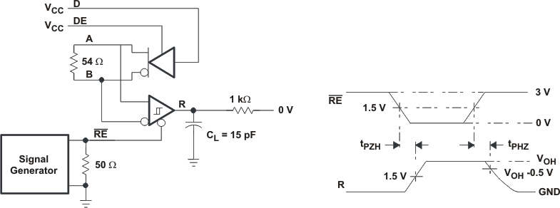 Figure 7-10 Receiver
Enable and Disable Test Circuit and Waveforms, Data Output High
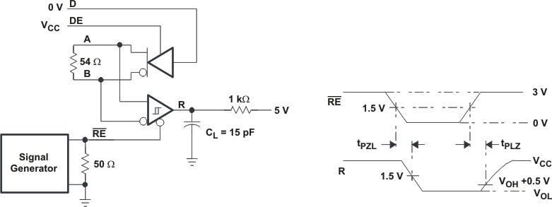 Figure 7-11 Receiver
Enable and Disable Test Circuit and Waveforms, Data Output Low
 Figure 7-12 Receiver
Enable From Shutdown Test Circuit and Waveforms
 Figure 7-13 Test
Circuit and Waveforms, Transient Overvoltage Test
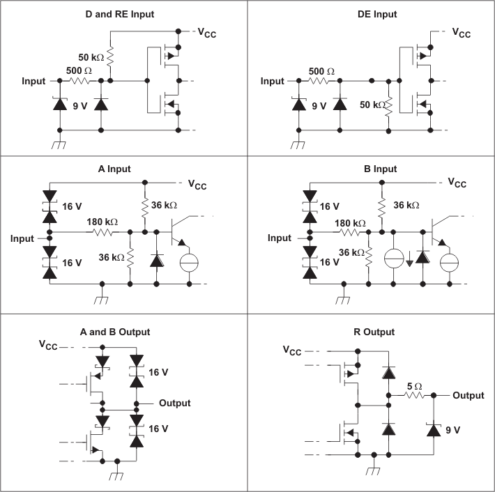 Figure 7-14 Equivalent Input and Output Schematic Diagrams