JAJSCH3 September 2016 SN65HVS883
PRODUCTION DATA.
- 1 特長
- 2 アプリケーション
- 3 概要
- 4 改訂履歴
- 5 Pin Configuration and Functions
- 6 Specifications
- 7 Parameter Measurement Information
- 8 Detailed Description
- 9 Application and Implementation
- 10Power Supply Recommendations
- 11Layout
- 12デバイスおよびドキュメントのサポート
- 13メカニカル、パッケージ、および注文情報
9 Application and Implementation
NOTE
Information in the following applications sections is not part of the TI component specification, and TI does not warrant its accuracy or completeness. TI’s customers are responsible for determining suitability of components for their purposes. Customers should validate and test their design implementation to confirm system functionality.
9.1 Application Information
9.1.1 System-Level EMC
The SN65HVS883 must operate reliably in harsh industrial environments. At a system level, the device is tested according to several international electromagnetic compatibility (EMC) standards.
In addition to the device internal ESD structures, external protection circuitry, such as the one in Figure 17, can be used to absorb as much energy from burst- and surge-transients as possible.
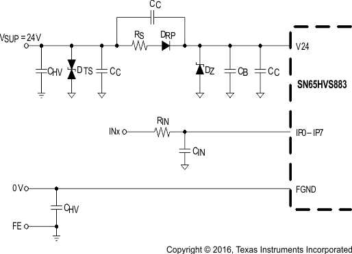 Figure 17. Typical EMC Protection Circuitry for Supply and Signal Inputs
Table 3. Components
| DESIGNATOR | DESCRIPTION |
|---|---|
| DTS | 39 V Transient Voltage Suppressor: SM15T39CA |
| DRP | Super Rectifier: BYM10-1000, or General Purpose rectifier: 1N4007 |
| DZ | 33 V – 36 V fast Zener Diode, Z2SMB36 |
| RS | 56 Ω, 1/3 W MELF Resistor |
| RIN | 1.2 kΩ, 1/4 W MELF Resistor |
| CIN | 22 nF, 60 V Ceramic Capacitor |
| CHV | 4.7 nF, 2 kV Ceramic Capacitor |
| CC | n x 220 nF, 60 V Ceramic Capacitors |
| CB | 1 µF - 10 µF, 60 V Ceramic Capacitor |
9.1.2 Input Channel Switching Characteristics
The input stage of the SN65HVS883 is so designed, that for an input resistor RIN = 1.2 kΩ the trip point for signalling an ON-condition is at 9.4 V at 3.6 mA. This trip point satisfies the switching requirements of IEC61131-2 Type 1 and Type 3 switches.
 Figure 18. Switching Characteristics for IEC61131-2 Type 1, 2, and 3 Proximity Switches
For a Type 2 switch application, two inputs are connected in parallel. The current limiters then add to a total maximum current of 7.2 mA. While the return-path (RE-pin), of one input might be used to drive an indicator LED, the RE-pin of the other input channel should be connected to ground (FGND).
Paralleling input channels reduces the number of available input channels from an octal Type 1 or Type 3 input to a quad Type 2 input device. Note, that in this configuration output data of an input channel is represented by two shift register bits.
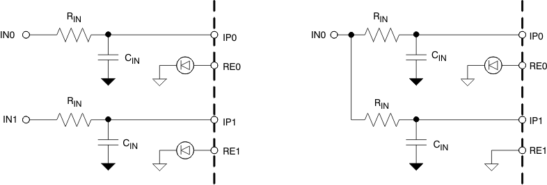 Figure 19. Paralleling Two Type 1 or Type 3 Inputs Into One Type 2 Input
9.1.3 Digital Interface Timing
The digital interface of the SN65HVS883 is SPI compatible and interfaces, isolated or non-isolated, to a wide variety of standard micro controllers.
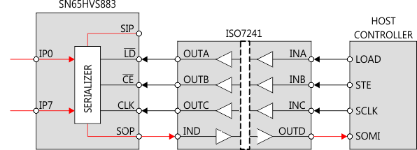 Figure 20. Simple Isolation of the Shift Register Interface
Upon a low-level at the load input, LD, the information of the field inputs, IP0 to IP7 is latched into the shift register. Taking LD high again blocks the parallel inputs of the shift register from the field inputs. A low-level at the clock-enable input, CE, enables the clock signal, CLK, to serially shift the data to the serial output, SOP. Data is clocked into the shift register at the rising edge of CLK and out of the shift register on the falling edge of CLK. Thus after eight consecutive clock cycles all field input data have been clocked out of the shift register and the information of the serial input, SIP, appears at the serial output, SOP.
The CE signal should only be transitioned low while the CLK signal is low which ensures that a rising edge of CLK occurs before a falling edge of CLK. This shifts the data into and through the shift register up until the final register before the first bit that was loaded into the final register is shifted out the serial output, SOP. If a falling edge of CLK is seen first following the transition of CE to low, the final register outputs the first bit, IP0, on the serial output, SOP, before shifting the rest of the bits through the shift register. The previous value of the second to last register prior to the LD event will then be shifted into the final register on the next rising CLK edge and output on the serial output, SOP, before the next valid bit, IP1, is output on the serial output, SOP. This appears as an erroneous bit in the serial data. Also, depending on how many falling CLK edges were seen before the CE signal is transitioned back high, the final bit, IP7, may not get shifted out of the shift register.
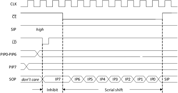 Figure 21. Interface Timing for Parallel-Load and Serial-Shift Operation of the Shift Register
9.1.4 Cascading for High Channel Count Input Modules
Designing high-channel count modules require cascading multiple SN65HVS883 devices. Simply connect the serial output (SOP) of a leading device with the serial input (SIP) of a following device without changing the processor interface.
 Figure 22. Cascading Four SN65HVS883 for a 32-Channel Input Module
NOTE
When daisy-chaining multiple devices, the maximum operating rate (CLK pulse width) may need to be restricted in order to maintain minimum set-up/hold timing relationships between the serial data (SIP/SOP) and the CLK line.
9.2 Typical Application
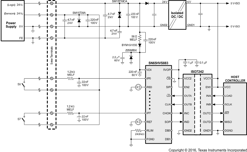 Figure 23. Typical Digital Input Module Application
9.2.1 Design Requirements
The simplified schematic in Figure 23 demonstrates a typical application of the SN65HVS883 for sensing the state of digital switches with 24-V high logic levels. In this application, a 5-V host controller must receive the state of 8 switches as a serial input, while remaining isolated from the high voltage power supply.
9.2.2 Detailed Design Procedure
9.2.2.1 Input Stage
Selection of the current limiting resistor RLIM sets the input current limit ILIM for the device. Digital Inputs includes necessary equations for choosing the limiting resistor.
The On/Off voltage thresholds at the device pin VTH(IP+) and VTH(IP-) are fixed to 5.2 V and 4.3 V respectively, however the On/Off voltage thresholds of the field input VTH(IN+) and VTH(IN-) are determined by the value of the series resistor RIN placed between the field input and the device. The threshold voltage VTH(IN+) is determined with the following equation:

Substituting Equation 1 and solving for RIN produces an equation for RIN given a desired on-threshold.

The following equation can be used to calculate the off-threshold voltage given a value for RIN

Figure 24 contains an example input characteristic:
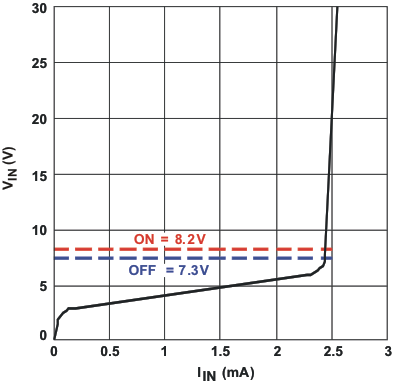 Figure 24. SN65HVS883 Example Input Characteristic
9.2.2.2 Setting Debounce Time
The logic signals at the DB0 and DB1 pins determine the denounce times for the device according to the table in section 6.5. The DB0 and DB1 pins are internally pulled high. Connecting the pins to GND in different configurations allows for selection of 0, 1, or 3 ms debounce times. In noisy environments, it is recommended that unused DB pins should be connected externally to a 5 V supply.
9.2.2.3 Example: High-Voltage Sensing Application
For the high-voltage sensing application in Figure 23, inputs from each switch (S0-S7) are connected to the 8 parallel inputs (IP0-IP7) of the SN65HVS883 through 1.2 kΩ MELF resistors. Small capacitors (22 nF) are tied to ground at each input to provide noise protection for the signals. A resistor is added between the RLIM pin and GND to provide a device current limit according to the equation ILIM = 90 V / RLIM. In this example, with a 24.9 kΩ resistor, the current limit for the device is set to 3.6 mA. LEDs are placed between pins RE0-RE7 to allow for external status observation of the parallel inputs. Finally the SN65HVS883 is connected through a digital isolation device to the host controller to provide galvanic isolation to the external interfaces and to allow for communication between the 5 V SN65HVS883 logic and the 5-V host controller. The host controller manages mode switching and clocking of the SN65HVS883 through the digital isolation device.
9.2.3 Application Curve
The application traces acquired in Figure 25 demonstrates the typical behavior of the SN65HVD883 when in shift mode (Load Pulse Input pulled high and Clock Enable Input pulled low). Channel 1 shows the SIP input, Channel 2 shows the CLK input, and Channel 3 shows the SOP output.
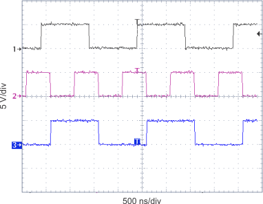 Figure 25. SN65HVS883 Serial Input and Output Timing