JAJSGX8C April   2002  – February 2019 SN65LVDT14 , SN65LVDT41

PRODUCTION DATA.  

  1. 特長
  2. アプリケーション
  3. 概要
    1.     Device Images
      1.      SN65LVDT41 の機能図
      2.      SN65LVDT14 の機能図
  4. 改訂履歴
  5. 概要(続き)
  6. Pin Configuration and Functions
    1.     SN65LVDT41 Pin Functions
    2.     SN65LVDT14 Pin Functions
  7. Specifications
    1. 7.1  Absolute Maximum Ratings
    2. 7.2  ESD Ratings
    3. 7.3  Recommended Operating Conditions
    4. 7.4  Thermal Information
    5. 7.5  Receiver Electrical Characteristics
    6. 7.6  Driver Electrical Characteristics
    7. 7.7  Device Electrical Characteristics
    8. 7.8  Receiver Switching Characteristics
    9. 7.9  Driver Switching Characteristics
    10. 7.10 Typical Characteristics
      1. 7.10.1 Receiver
      2. 7.10.2 Driver
  8. Parameter Measurement Information
  9. Detailed Description
    1. 9.1 Overview
    2. 9.2 Functional Block Diagram
    3. 9.3 Feature Description
      1. 9.3.1 SN65LVDTxx Driver and Receiver Functionality
      2. 9.3.2 Integrated Termination
      3. 9.3.3 SN65LVDTxx Equivalent Circuits
    4. 9.4 Device Functional Modes
  10. 10Application and Implementation
    1. 10.1 Application Information
      1. 10.1.1 Extending a Serial Peripheral Interface Using LVDS Signaling Over Differential Transmission Cables
    2. 10.2 Typical Application
      1. 10.2.1 Design Requirements
      2. 10.2.2 Detailed Design Procedure
        1. 10.2.2.1 SPI Propagation Delay Limitations
        2. 10.2.2.2 Interconnecting Media
        3. 10.2.2.3 Input Fail-Safe Biasing
        4. 10.2.2.4 Power Decoupling Recommendations
        5. 10.2.2.5 PCB Transmission Lines
        6. 10.2.2.6 Probing LVDS Transmission Lines on PCB
      3. 10.2.3 Application Curve
  11. 11Power Supply Recommendations
  12. 12Layout
    1. 12.1 Layout Guidelines
      1. 12.1.1 Microstrip vs. Stripline Topologies
      2. 12.1.2 Dielectric Type and Board Construction
      3. 12.1.3 Recommended Stack Layout
      4. 12.1.4 Separation Between Traces
      5. 12.1.5 Crosstalk and Ground Bounce Minimization
      6. 12.1.6 Decoupling
    2. 12.2 Layout Examples
  13. 13デバイスおよびドキュメントのサポート
    1. 13.1 関連資料
    2. 13.2 ドキュメントの更新通知を受け取る方法
    3. 13.3 関連リンク
    4. 13.4 コミュニティ・リソース
    5. 13.5 商標
    6. 13.6 静電気放電に関する注意事項
    7. 13.7 Glossary
  14. 14メカニカル、パッケージ、および注文情報

パッケージ・オプション

デバイスごとのパッケージ図は、PDF版データシートをご参照ください。

メカニカル・データ(パッケージ|ピン)
  • PW|20
サーマルパッド・メカニカル・データ
発注情報

Microstrip vs. Stripline Topologies

As per the LVDS application and data handbook (SLLD009), printed-circuit boards usually offer designers two transmission line options: microstrip and stripline. Microstrips are traces on the outer layer of a PCB, as shown in Figure 23.
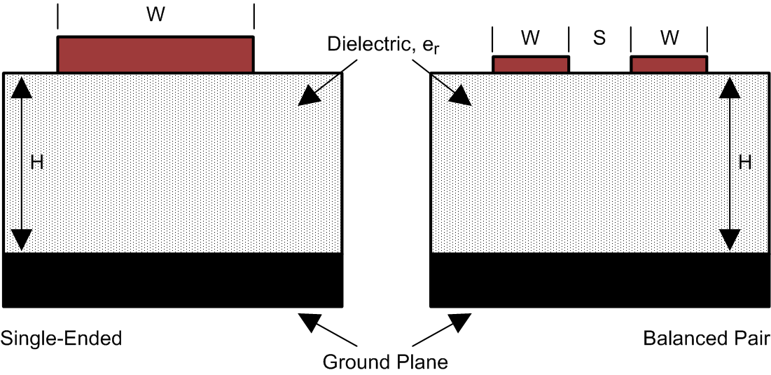
SN65LVDT14 SN65LVDT41 lo_mt_slls373.pngFigure 23. Microstrip Topology

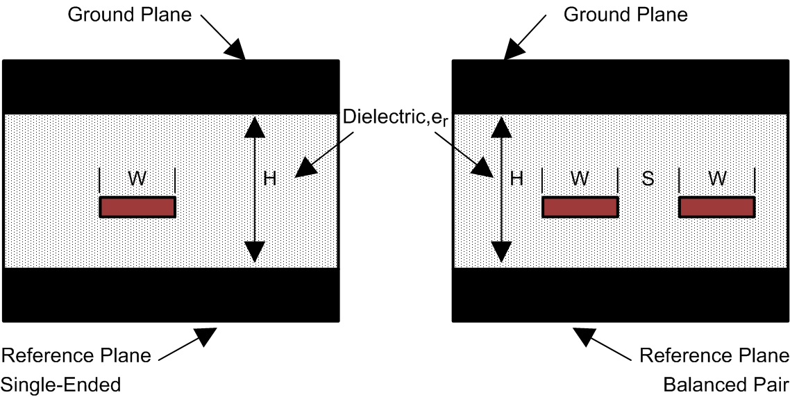
On the other hand, striplines are traces between two ground planes. Striplines are less prone to emissions and susceptibility problems because the reference planes effectively shield the embedded traces. However, from the standpoint of high-speed transmission, juxtaposing two planes creates additional capacitance. TI recommends routing LVDS signals on microstrip transmission lines when possible. The PCB traces allow designers to specify the necessary tolerances for ZO based on the overall noise budget and reflection allowances. Footnotes 1(2), 2(3), and 3(4) provide formulas for ZO and tPD for differential and single-ended traces. (2)(3)(4)
Howard Johnson & Martin Graham.1993. High Speed Digital Design – A Handbook of Black Magic. Prentice Hall PRT. ISBN number 013395724.
Mark I. Montrose. 1996. Printed Circuit Board Design Techniques for EMC Compliance. IEEE Press. ISBN number 0780311310.
Clyde F. Coombs, Jr. Ed, Printed Circuits Handbook, McGraw Hill, ISBN number 0070127549.

SN65LVDT14 SN65LVDT41 lo_st_slls373.pngFigure 24. Stripline Topology