SCLS226K October 1995 – July 2014 SN54AHC244 , SN74AHC244
PRODUCTION DATA.
- 1 Features
- 2 Applications
- 3 Description
- 4 Simplified Schematic
- 5 Revision History
- 6 Pin Configuration and Functions
- 7 Specifications
- 8 Parameter Measurement Information
- 9 Detailed Description
- 10Application and Implementation
- 11Power Supply Recommendations
- 12Layout
- 13Device and Documentation Support
- 14Mechanical, Packaging, and Orderable Information
パッケージ・オプション
デバイスごとのパッケージ図は、PDF版データシートをご参照ください。
メカニカル・データ(パッケージ|ピン)
- DGV|20
- DB|20
- NS|20
- N|20
- DW|20
- PW|20
サーマルパッド・メカニカル・データ
- PW|20
発注情報
9 Detailed Description
9.1 Overview
The SNx4AHC244 devices are organized as two 4-bit buffers/line drivers with separate output-enable (OE) inputs. When OE is low, the device passes data from the A inputs to the Y outputs. When OE is high, the outputs are in the high-impedance state. To ensure the high-impedance state during power up or power down, OE should be tied to VCC through a pullup resistor; the minimum value of the resistor is determined by the current-sinking capability of the driver.
9.2 Functional Block Diagram
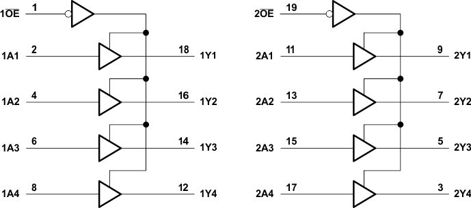 Figure 4. Logic Diagram (Positive Logic)
9.3 Feature Description
- VCC is optimized at 5 V
- Allows down voltage translation
- Inputs accept VIH levels of 5.5 V
- Slow edge rates minimize output ringing
9.4 Device Functional Modes
Table 1. Function Table
(Each 4-Bit Buffer/Driver)
| INPUTS | OUTPUT Y |
|
|---|---|---|
| OE | A | |
| L | H | H |
| L | L | L |
| H | X | Z |