SCES587D AUGUST 2004 – November 2015 SN74AVCH16T245
PRODUCTION DATA.
- 1 Features
- 2 Applications
- 3 Description
- 4 Revision History
- 5 Description (continued)
- 6 Pin Configuration and Functions
-
7 Specifications
- 7.1 Absolute Maximum Ratings
- 7.2 ESD Ratings
- 7.3 Recommended Operating Conditions
- 7.4 Thermal Information
- 7.5 Electrical Characteristics
- 7.6 Switching Characteristics: VCCA = 1.2 V
- 7.7 Switching Characteristics: VCCA = 1.5 V ± 0.1 V
- 7.8 Switching Characteristics: VCCA = 1.8 V ± 0.15 V
- 7.9 Switching Characteristics: VCCA = 2.5 V ± 0.2 V
- 7.10 Switching Characteristics: VCCA = 3.3 V ± 0.3 V
- 7.11 Operating Characteristics
- 7.12 Typical Characteristics (TA = 25°C)
- 8 Parameter Measurement Information
- 9 Detailed Description
- 10Application and Implementation
- 11Power Supply Recommendations
- 12Layout
- 13Device and Documentation Support
- 14Mechanical, Packaging, and Orderable Information
パッケージ・オプション
デバイスごとのパッケージ図は、PDF版データシートをご参照ください。
メカニカル・データ(パッケージ|ピン)
- DGG|48
- DGV|48
サーマルパッド・メカニカル・データ
発注情報
9 Detailed Description
9.1 Overview
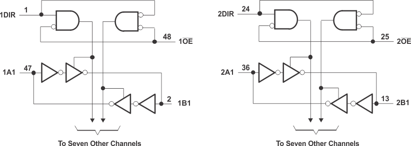
The SN74AVCH16T245 is a 16-bit, dual-supply noninverting bidirectional voltage level translation. Pins A and control pins (DIR and OE) are supported by VCCA and pins B are supported by VCCB. The A port can accept I/O voltages ranging from 1.2 V to 3.6 V, while the B port can accept I/O voltages from 1.2 V to 3.6 V. A high on DIR allows data transmission from A to B and a low on DIR allows data transmission from B to A when OE is set to low. When OE is set to high, both A and B are in the high-impedance state.
SN74AVCH16T245 features Active bus-hold circuitry holds unused or undriven inputs at a valid logic state. Use of pullup or pulldown resistors with the bus-hold circuitry is not recommended.
This device is fully specified for partial-power-down applications using off output current ( Ioff).
The VCC isolation feature ensures that if either VCC input is at GND, both ports are put in a high-impedance state.
9.2 Functional Block Diagram

9.3 Feature Description
9.3.1 Fully Configurable Dual-Rail Design Allows Each Port to Operate Over the Full 1.2 V to 3.6 V Power-Supply Range
Both VCCA and VCCB can be supplied at any voltage from 1.2 V to 3.6 V making the device suitable for translating between any of the low voltage nodes (1.2 V, 1.8 V, 2.5 V, and 3.3 V).
9.3.2 Partial-Power-Down Mode Operation
The Ioff circuitry will prevent backflow current by disabling I/O output circuits when device is in partial power-down mode. This device is fully specified for partial-power-down applications using off output current (Ioff). The Ioff circuitry disables the outputs, preventing damaging current backflow through the device when it is powered down.
9.3.3 VCC Isolation
The VCC isolation feature ensures that if either VCCA or VCCB are at GND, both ports will be in a high-impedance state (IOZ shown in Electrical Characteristics). This prevents false logic levels from being presented to either bus.
9.4 Device Functional Modes
The SN74AVCH16T245 is a voltage level translator that can operate from 1.2 V to 3.6 V (VCCA) and 1.2 V to 3.6 V (VCCB). The signal translation between 1.2 V and 3.6 V requires direction control and output enable control. When OE is low and DIR is high, data transmission is from A to B. When OE is low and DIR is low, data transmission is from B to A. When OE is high, both output ports will be high-impedance.
Table 1. Function Table
(Each Transceiver)
| INPUTS | OPERATION | |
|---|---|---|
| OE | DIR | |
| L | L | B data to A bus |
| L | H | A data to B bus |
| H | X | Isolation |
Table 2. Typical Total Static Power Consumption (ICCA + ICCB)
| VCCB | VCCA | UNIT | |||||
|---|---|---|---|---|---|---|---|
| 0 V | 1.2 V | 1.5 V | 1.8 V | 2.5 V | 3.3 V | ||
| 0 V | 0 | < 0.5 | < 0.5 | < 0.5 | < 0.5 | < 0.5 | μA |
| 1.2 V | < 0.5 | < 1 | < 1 | < 1 | < 1 | 1 | |
| 1.5 V | < 0.5 | < 1 | < 1 | < 1 | < 1 | 1 | |
| 1.8 V | < 0.5 | < 1 | < 1 | < 1 | < 1 | < 1 | |
| 2.5 V | < 0.5 | 1 | < 1 | < 1 | < 1 | < 1 | |
| 3.3 V | < 0.5 | 1 | < 1 | < 1 | < 1 | < 1 | |