SDLS020F May 1990 – July 2016 SN54LS06 , SN74LS06
PRODUCTION DATA.
- 1 Features
- 2 Applications
- 3 Description
- 4 Revision History
- 5 Pin Configuration and Functions
- 6 Specifications
- 7 Parameter Measurement Information
- 8 Detailed Description
- 9 Application and Implementation
- 10Power Supply Recommendations
- 11Layout
- 12Device and Documentation Support
- 13Mechanical, Packaging, and Orderable Information
パッケージ・オプション
メカニカル・データ(パッケージ|ピン)
サーマルパッド・メカニカル・データ
- D|14
発注情報
11 Layout
11.1 Layout Guidelines
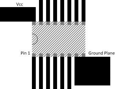
When using multiple bit logic devices, inputs must not ever float. In many cases, functions or parts of functions of digital logic devices are unused; for example, when only two inputs of a triple-input and gate are used or only 3 of the 4 buffer gates are used. Such input pins must not be left unconnected because the undefined voltages at the outside connections result in undefined operational states. The following rules must be observed under all circumstances. All unused inputs of digital logic devices must be connected to a high or low bias to prevent them from floating. The logic level that must be applied to any particular unused input depends on the function of the device. Generally they are tied to GND or VCC whichever make more sense or is more convenient. TI recommends keeping the signal lines as short and as straight as possible (see Figure 6). Incorporation of microstrip or stripline techniques are also recommended when signal lines are more than 1" long. These traces must be designed with a characteristic impedance of either 50 Ω or 75 Ω as required by the application.
11.2 Layout Examples
 Figure 5. Layout Schematic
 Figure 6. Signal Line Layout