SDLS021D May 1990 – April 2016 SN74LS07
PRODUCTION DATA.
- 1 Features
- 2 Applications
- 3 Description
- 4 Revision History
- 5 Pin Configuration and Functions
- 6 Specifications
- 7 Parameter Measurement Information
- 8 Detailed Description
- 9 Application and Implementation
- 10Power Supply Recommendations
- 11Layout
- 12Device and Documentation Support
- 13Mechanical, Packaging, and Orderable Information
パッケージ・オプション
デバイスごとのパッケージ図は、PDF版データシートをご参照ください。
メカニカル・データ(パッケージ|ピン)
- D|14
- DB|14
- N|14
- NS|14
サーマルパッド・メカニカル・データ
- D|14
発注情報
9 Application and Implementation
NOTE
Information in the following applications sections is not part of the TI component specification, and TI does not warrant its accuracy or completeness. TI’s customers are responsible for determining suitability of components for their purposes. Customers should validate and test their design implementation to confirm system functionality.
9.1 Application Information
The SN74LS07 device is a high-drive, open-drain CMOS device that can be used for a multitude of buffer-type functions. It can produce 40 mA of drive current at 5 V. Therefore, this device is ideal for driving multiple inputs. The inputs are 5.25-V tolerant and outputs are 30-V tolerant.
9.2 Typical Application
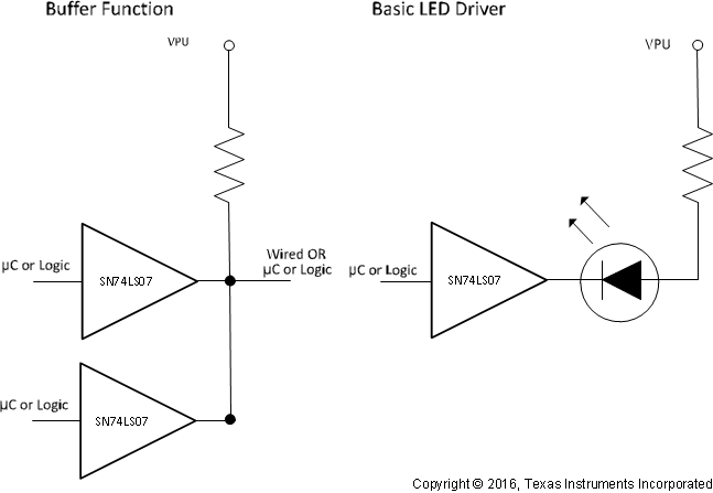
Multiple channels of the SN74LS07 device can be used to create a positive AND logic function, as shown in Figure 4. Additionally, the SN74LS07 device can be used to drive an LED by sinking up to 40 mA, which may be more than the previous stage can sink.
 Figure 4. Typical Application Diagram
9.2.1 Design Requirements
Ensure that the inputs are in a known state as defined by VIH and VIL noted in Recommended Operating Conditions, or else the outputs may be in an unknown state.
9.2.2 Detailed Design Procedure
- Recommended Input Conditions
- For specified high and low level, see VIH and VIL in Recommended Operating Conditions.
- Inputs are overvoltage tolerant allowing them to go as high as 5.25 V.
- Recommend Output Conditions
- Load currents must not exceed 40 mA per output.
- Outputs must not be pulled above 30 V.
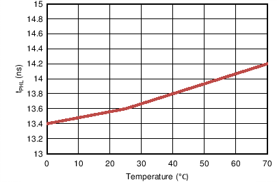
9.2.3 Application Curve
