SCES337K May 2000 – October 2014 SN74LV07A
PRODUCTION DATA.
- 1 Features
- 2 Applications
- 3 Description
- 4 Simplified Schematic
- 5 Revision History
- 6 Pin Configuration and Functions
-
7 Specifications
- 7.1 Absolute Maximum Ratings
- 7.2 Handling Ratings
- 7.3 Recommended Operating Conditions
- 7.4 Thermal Information
- 7.5 Electrical Characteristics
- 7.6 Switching Characteristics, VCC = 2.5 V ± 0.2 V
- 7.7 Switching Characteristics, VCC = 3.3 V ± 0.3 V
- 7.8 Switching Characteristics, VCC = 5 V ± 0.5 V
- 7.9 Noise Characteristics
- 7.10 Operating Characteristics
- 7.11 Typical Characteristics
- 8 Parameter Measurement Information
- 9 Detailed Description
- 10Application and Implementation
- 11Power Supply Recommendations
- 12Layout
- 13Device and Documentation Support
- 14Mechanical, Packaging, and Orderable Information
パッケージ・オプション
デバイスごとのパッケージ図は、PDF版データシートをご参照ください。
メカニカル・データ(パッケージ|ピン)
- D|14
- DGV|14
- DB|14
- PW|14
- NS|14
サーマルパッド・メカニカル・データ
- PW|14
発注情報
9 Detailed Description
9.1 Overview
The outputs of the SN74LV07A device are open drain and can be connected to other open-drain outputs to implement active-low wired-OR or active-high wired-AND functions. The maximum sink current is 16 mA at
5-V VCC. Inputs can be driven from 2.5-V, 3.3-V, or 5-V (CMOS) devices. This feature allows the use of the SN74LV07A device as a translator in a mixed-system environment. This device is fully specified for partial power-down applications using Ioff. The Ioff circuitry disables the outputs, thus preventing a damaging current backflow through the device when it is powered down.
9.2 Functional Block Diagram
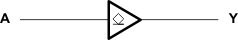 Figure 4. Logic Diagram, Each Buffer/Driver (Positive Logic)
9.3 Feature Description
- Wide operating voltage range
- Operates from 2 V to 5.5 V
- Allows up or down voltage translation
- Inputs and outputs accept voltages to 5.5 V
- Ioff feature
- Allows voltages on the inputs and outputs when VCC is 0 V
9.4 Device Functional Modes
Table 1. Function Table
(Each Buffer/Driver)
| INPUT A |
OUTPUT Y |
|---|---|
| H | H |
| L | L |