JAJST70J April 1999 – February 2024 SN74LV4066A
PRODUCTION DATA
- 1
- 1 特長
- 2 アプリケーション
- 3 概要
- 4 Pin Configuration and Functions
-
5 Specifications
- 5.1 Absolute Maximum Ratings
- 5.2 ESD Ratings
- 5.3 Thermal Information: SN74LV4066A
- 5.4 Recommended Operating Conditions
- 5.5 Electrical Characteristics (LV)
- 5.6 Timing Characteristics VCC = 2.5V ± 0.2V
- 5.7 Timing Characteristics VCC = 3.3V ± 0.3V
- 5.8 Timing Characteristics VCC = 5V ± 0.5V
- 5.9 AC Characteristics
- 6 Parameter Measurement Information
- 7 Detailed Description
- 8 Device and Documentation Support
- 9 Revision History
- 10Mechanical, Packaging, and Orderable Information
パッケージ・オプション
デバイスごとのパッケージ図は、PDF版データシートをご参照ください。
メカニカル・データ(パッケージ|ピン)
- D|14
- RGY|14
- DGV|14
- DB|14
- PW|14
- N|14
- NS|14
サーマルパッド・メカニカル・データ
発注情報
4 Pin Configuration and Functions
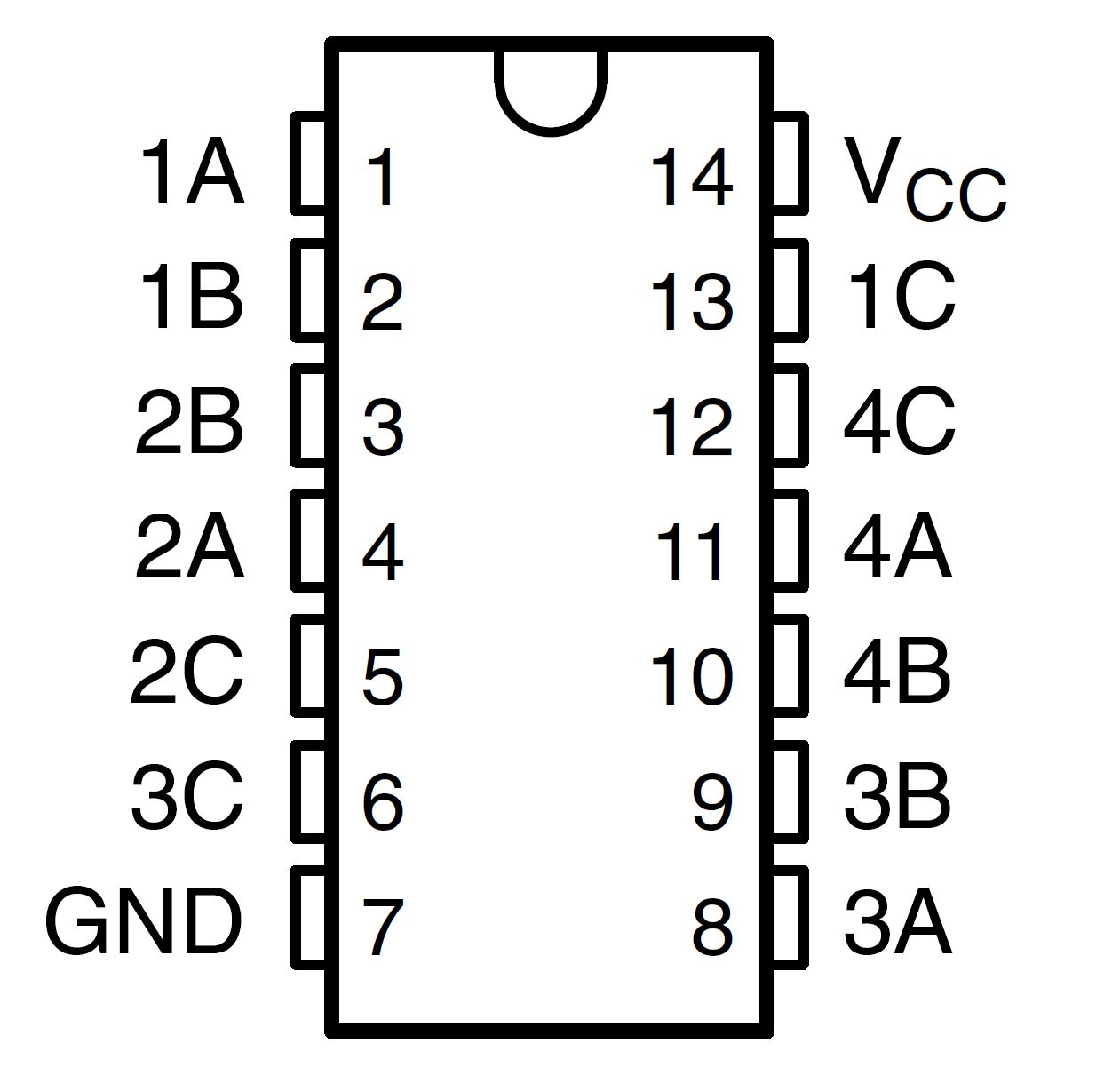
 Figure 4-1 D or PW Package, 14-Pin SOIC or
TSSOP (Top View)
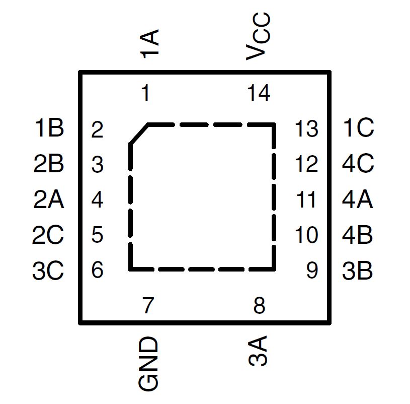
 Figure 4-2 RGY Package, 14- Pin QFN (Top
View)
Figure 4-2 RGY Package, 14- Pin QFN (Top
View)Table 4-1 Pin Functions
| PIN | TYPE(1) | DESCRIPTION | |
|---|---|---|---|
| NAME | NO. | ||
| 1A | 1 | I/O | Input/Output to switch channel 1 |
| 1B | 2 | I/O | Input/Output to switch channel 1 |
| 2B | 3 | I/O | Input/Output to switch channel 2 |
| 2A | 4 | I/O | Input/Output to switch channel 2 |
| 2C | 5 | I | Control line for channel 2. Switch is ON when control pin is high. |
| 3C | 6 | I | Control line for channel 3. Switch is ON when control pin is high. |
| GND | 7 | — | Ground (0V) reference |
| 3A | 8 | I/O | Input/Output to switch channel 3 |
| 3B | 9 | I/O | Input/Output to switch channel 3 |
| 4B | 10 | I/O | Input/Output to switch channel 4 |
| 4A | 11 | I/O | Input/Output to switch channel 4 |
| 4C | 12 | I | Control line for channel 4. Switch is ON when control pin is high. |
| 1C | 13 | I | Control line for channel 1. Switch is ON when control pin is high. |
| VCC | 14 | — | Positive power supply. This pin is the most positive power-supply potential. For reliable operation, connect a decoupling capacitor ranging from 0.1µF to 10µF between VDD and GND. |
| Thermal pad | — | It is recommended to tie the pad to GND for the best performance. | |
(1) Signal types: I = input, O = output, I/O
= input or output.