JAJSHV2E April 2003 – August 2020 SN74LVC1G125-Q1
PRODUCTION DATA
- 1 特長
- 2 アプリケーション
- 3 概要
- 4 Revision History
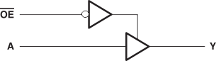
- 5 Pin Configuration and Functions
- 6 Specifications
- 7 Parameter Measurement Information
- 8 Detailed Description
- 9 Application and Implementation
- 10Power Supply Recommendations
- 11Layout
- 12Device and Documentation Support
- 13Mechanical, Packaging, and Orderable Information
パッケージ・オプション
デバイスごとのパッケージ図は、PDF版データシートをご参照ください。
メカニカル・データ(パッケージ|ピン)
- DBV|5
- DCK|5
- DRY|6
サーマルパッド・メカニカル・データ
- DRY|6
発注情報
3 概要
このバス・バッファ・ゲートは、1.65V~5.5V の VCC で動作するように設計されています。
SN74LVC1G125-Q1 は、3 ステート出力に対応したシングル・ライン・ドライバです。出力イネーブル (OE) 入力が HIGH になると、出力はディセーブルされます。
このCMOS デバイスは出力駆動能力が大きく、広い VCC 動作範囲にわたって静止電力消費が低く保たれます。
SN74LVC1G125-Q1 は、本体サイズ 1.45mm × 1.00mm の小型 DRY パッケージなど、各種のパッケージで供給されます。
製品情報
| 型番 | パッケージ(1) | 本体サイズ (公称) |
|---|---|---|
| CLVC1G125QDBVRQ1 | SOT-23 (5) | 2.90mm × 1.60mm |
| 1P1G125QDCKRQ1 | SC70 (5) | 2.00mm × 1.25mm |
| 1P1G125QDRYRQ1 | SON (6) | 1.45mm × 1.00mm |
(1) 利用可能なすべてのパッケージについては、このデータシートの末尾にある注文情報を参照してください。