JAJSD25 March 2017 SN74LVC1G79-Q1
PRODUCTION DATA.
- 1 特長
- 2 アプリケーション
- 3 概要
- 4 改訂履歴
- 5 Pin Configuration and Functions
-
6 Specifications
- 6.1 Absolute Maximum Ratings
- 6.2 ESD Ratings
- 6.3 Recommended Operating Conditions
- 6.4 Thermal Information
- 6.5 Electrical Characteristics
- 6.6 Timing Requirements: TA = -40°C to +85°C
- 6.7 Timing Requirements: TA = -40°C to +125°C
- 6.8 Switching Characteristics: CL = 15 pF, TA = -40°C to +85°C
- 6.9 Switching Characteristics: CL = 30 or 50 pF, TA = -40°C to +85°C
- 6.10 Switching Characteristics: CL = 30 pF or 50 pF, TA = -40°C to +125°C
- 6.11 Operating Characteristics
- 6.12 Typical Characteristics
- 7 Parameter Measurement Information
- 8 Detailed Description
- 9 Application and Implementation
- 10Power Supply Recommendations
- 11Layout
- 12デバイスおよびドキュメントのサポート
- 13メカニカル、パッケージ、および注文情報
9 Application and Implementation
NOTE
Information in the following applications sections is not part of the TI component specification, and TI does not warrant its accuracy or completeness. TI’s customers are responsible for determining suitability of components for their purposes. Customers should validate and test their design implementation to confirm system functionality.
9.1 Application Information
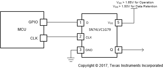
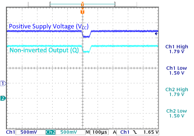
A useful application for the SN74LVC1G79-Q1 is using it as a data latch with low-voltage data retention. This application implements the use of a microcontroller GPIO pin to act as a clock to set the output state and a second GPIO to provide the input data. If the SN74LVC1G79-Q1 is being powered from 1.8 V and there is concern that a power glitch could exist as low as 1.5 V, the device will retain the state of the Q output. An example of this data retention is shown in Figure 8 where the VCC drops to 1.5 V and the Q output maintains the HIGH output state when VCC returns to 1.8 V. If the VCC voltage drops below 1.5 V, data retention is not guaranteed.
9.2 Typical Application
 Figure 7. Low Voltage Data Retention With SN74LVC1G79-Q1
9.2.1 Design Requirements
The SN74LVC1G79-Q1 device uses CMOS technology and has balanced output drive. Take care to avoid bus contention because it can drive currents that would exceed maximum limits.
9.2.2 Detailed Design Procedure
- Recommended input conditions:
- For rise time and fall time specifications, see Δt/Δv in Recommended Operating Conditions.
- For specified high and low levels, see VIH and VIL in Recommended Operating Conditions.
- Input voltages are recommended to not go below 0 V and not exceed 5.5 V for any VCC. See Recommended Operating Conditions.
- Recommended output conditions:
- Load currents should not exceed ±50 mA. See Absolute Maximum Ratings.
- Output voltages are recommended to not go below 0 V and not exceed the VCC voltage. See Recommended Operating Conditions.
9.2.3 Application Curve
 Figure 8. Data Retention With VCC Glitch Down to 1.5 V