JAJSP71M December 2003 – October 2022 SN74LVC2T45
PRODUCTION DATA
- 1 特長
- 2 アプリケーション
- 3 概要
- 4 Revision History
- 5 Pin Configuration and Functions
-
6 Specifications
- 6.1 Absolute Maximum Ratings
- 6.2 ESD Ratings
- 6.3 Recommended Operating Conditions
- 6.4 Thermal Information
- 6.5 Electrical Characteristics
- 6.6 Switching Characteristics: VCCA = 1.8 V ± 0.15 V
- 6.7 Switching Characteristics: VCCA = 2.5 V ± 0.2 V
- 6.8 Switching Characteristics: VCCA = 3.3 V ± 0.3 V
- 6.9 Switching Characteristics: VCCA = 5 V ± 0.5 V
- 6.10 Operating Characteristics
- 6.11 Typical Characteristics
- 7 Parameter Measurement Information
- 8 Detailed Description
- 9 Application and Implementation
- 10Power Supply Recommendations
- 11Layout
- 12Device and Documentation Support
- 13Mechanical, Packaging, and Orderable Information
パッケージ・オプション
メカニカル・データ(パッケージ|ピン)
サーマルパッド・メカニカル・データ
発注情報
5 Pin Configuration and Functions
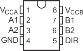
 Figure 5-1 DCT or DCU Package, 8-Pin SM8 or VSSOP (Top View)
Table 5-1 Pin Functions: DCT, DCU
| PIN | TYPE(1) | DESCRIPTION | |
|---|---|---|---|
| NAME | NO. | ||
| VCCA | 1 | P | A-port supply voltage. 1.65 V ≤ VCCA ≤ 5.5 V |
| A1 | 2 | I/O | Input/output A1. Referenced to VCCA |
| A2 | 3 | I/O | Input/output A2. Referenced to VCCA |
| GND | 4 | G | Ground |
| DIR | 5 | I | Direction control signal |
| B2 | 6 | I/O | Input/output B2. Referenced to VCCB |
| B1 | 7 | I/O | Input/output B1. Referenced to VCCB |
| VCCB | 8 | P | B-port supply voltage. 1.65 V ≤ VCCB ≤ 5.5 V |
(1) I = input, O = output, P = power, G =ground
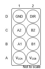
 Figure 5-2 YZP Package, 8-Pin DSGBA (Bottom View)
Table 5-2 Pin Functions: YZP
| PIN | TYPE(1) | DESCRIPTION | |
|---|---|---|---|
| NO. | NAME | ||
| A1 | VCCA | P | A-port supply voltage. 1.65 V ≤ VCCA ≤ 5.5 V |
| A2 | VCCB | P | B-port supply voltage. 1.65 V ≤ VCCB ≤ 5.5 V |
| B1 | A1 | I/O | Input/output A1. Referenced to VCCA |
| B2 | B1 | I/O | Input/output B1. Referenced to VCCB |
| C1 | A2 | I/O | Input/output A2. Referenced to VCCA |
| C2 | B2 | I/O | Input/output B2. Referenced to VCCB |
| D1 | GND | G | Ground |
| D2 | DIR | I | Direction control signal |
(1) I = input, O = output, P = power, G = ground