SLLSE57E April   2011  – March 2015 SN75DP130

PRODUCTION DATA.  

  1. Features
  2. Applications
  3. Description
  4. Revision History
  5. Description (continued)
  6. Pin Configuration and Functions
  7. Specifications
    1. 7.1 Absolute Maximum Ratings
    2. 7.2 ESD Ratings
    3. 7.3 Recommended Operating Conditions
    4. 7.4 Thermal Information
    5. 7.5 Power Dissipation
    6. 7.6 Electrical Characteristics
    7. 7.7 Switching Characteristics
    8. 7.8 Typical Characteristics
  8. Parameter Measurement Information
  9. Detailed Description
    1. 9.1 Overview
    2. 9.2 Functional Block Diagram
    3. 9.3 Feature Description
      1. 9.3.1 Reset Signal
      2. 9.3.2 Hot Plug Detect and Cable Adapter Detect
      3. 9.3.3 AUX and DDC Configuration
      4. 9.3.4 Main Link Configuration
      5. 9.3.5 Link Training and DPCD
      6. 9.3.6 Equalization
      7. 9.3.7 Configurable Outputs
      8. 9.3.8 Squelch
    4. 9.4 Device Functional Modes
    5. 9.5 Programming
      1. 9.5.1 I2C Interface Overview
    6. 9.6 Register Maps
      1. 9.6.1 SN75DP130 Local I2C Control and Status Registers
  10. 10Application and Implementation
    1. 10.1 Application Information
    2. 10.2 Typical Application
      1. 10.2.1 Design Requirements
      2. 10.2.2 Detailed Design Procedure
        1. 10.2.2.1 Logic I2C Interface
        2. 10.2.2.2 CAD Sink Over Ride
        3. 10.2.2.3 HPD Sink Over Ride
      3. 10.2.3 Application Curves
  11. 11Power Supply Recommendations
    1. 11.1 SN75DP130 Power Sequencing
      1. 11.1.1 Power-Up Sequence:
      2. 11.1.2 Power-Down Sequence:
  12. 12Layout
    1. 12.1 Layout Guidelines
      1. 12.1.1 Layer Stack
      2. 12.1.2 Differential Traces
    2. 12.2 Layout Example
  13. 13Device and Documentation Support
    1. 13.1 Trademarks
    2. 13.2 Electrostatic Discharge Caution
    3. 13.3 Glossary
  14. 14Mechanical, Packaging, and Orderable Information

パッケージ・オプション

メカニカル・データ(パッケージ|ピン)
サーマルパッド・メカニカル・データ
発注情報

11 Power Supply Recommendations

11.1 SN75DP130 Power Sequencing

The following power-up and power-down sequences describe how the RSTN signal is applied to the SN75DP130. See Power Dissipation.

11.1.1 Power-Up Sequence:

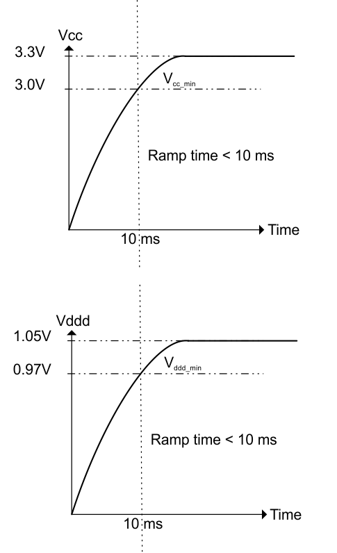
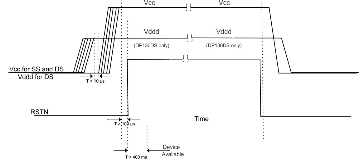
  1. Apply Vcc with less than a 10-ms ramp time for the SN75DP130 and for the SN75DP130, apply Vddd then Vcc (both having less than 10-ms ramp time) devices. Vddd must be asserted first and stable for greater than 10 µs before Vcc is applied.
  2. RSTN must remain asserted until Vcc/Vddd voltage has reached minimum recommended operation for more than 100 µs.
  3. De-assert RSTN (Note: This RSTN is a 1.05-V interface and is internally connected to Vddd_dreg through a 150-kΩ resistor).
  4. Device will be available for operation approximately 400 ms after a valid reset.

11.1.2 Power-Down Sequence:

  1. Assert RSTN to the device.
  2. Remove Vcc and Vddd.
SN75DP130 pwrup_pwrdwn_llse57.gifFigure 34. Power-Up and Power-Down Sequence
SN75DP130 vcc_ramp_recomendation_llse57.gifFigure 35. VCC/VDDD Ramp Recommendation
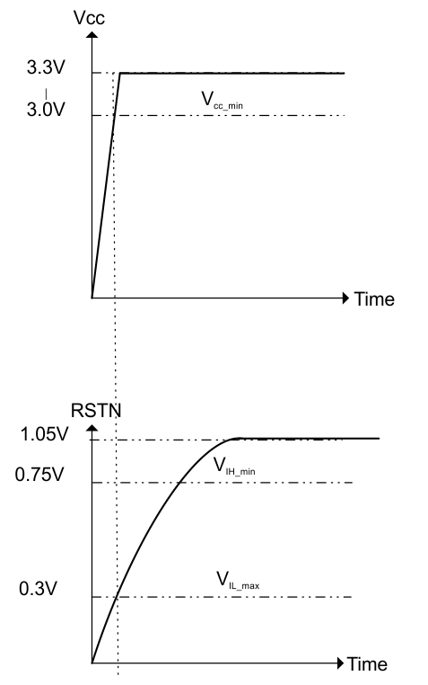
SN75DP130 rstn_voltage_thresholds_llse57.gifFigure 36. RSTN Voltage Thresholds