SLLS977F April 2009 – July 2017 SN75DP139
PRODUCTION DATA.
- 1 Features
- 2 Applications
- 3 Description
- 4 Revision History
- 5 Pin Configuration and Functions
-
6 Specifications
- 6.1 Absolute Maximum Ratings
- 6.2 ESD Ratings
- 6.3 Recommended Operating Conditions
- 6.4 Thermal Information
- 6.5 Electrical Characteristics (Device Power)
- 6.6 Electrical Characteristics (Hot Plug Detect)
- 6.7 Electrical Characteristics (Aux / I2C Pins)
- 6.8 Electrical Characteristics (TMDS and Main Link Pins)
- 6.9 Switching Characteristics (Hot Plug Detect)
- 6.10 Switching Characteristics (Aux / I2C Pins)
- 6.11 Switching Characteristics (TMDS and Main Link Pins)
- 6.12 Typical Characteristics
- 7 Detailed Description
- 8 Application and Implementation
- 9 Power Supply Recommendations
- 10Layout
- 11Device and Documentation Support
- 12Mechanical, Packaging, and Orderable Information
パッケージ・オプション
メカニカル・データ(パッケージ|ピン)
サーマルパッド・メカニカル・データ
発注情報
7 Detailed Description
7.1 Overview
The SN75DP139 is a Dual-Mode DisplayPort input to Transition-Minimized Differential Signaling (TMDS) output. The TMDS output has a built in level shifting re-driver supporting Digital Video Interface (DVI) 1.0 and High Definition Multimedia Interface (HDMI) 1.4b standards.
An integrated Active I2C buffer isolates the capacitive loading of the source system from that of the sink and interconnecting cable. This isolation improves overall signal integrity of the system and allows for considerable design margin within the source system for DVI / HDMI compliance testing.
A logic block was designed into the SN75DP139 in order to assist with TMDS connector identification. Through the use of the I2C_EN pin, this logic block can be enabled to indicate the translated port is an HDMI port; therefore legally supporting HDMI content.
7.2 Functional Block Diagram
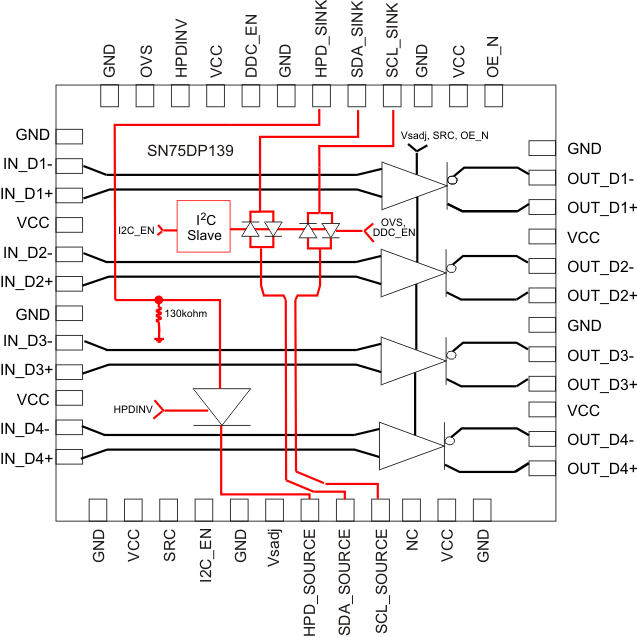 Figure 20. Data Flow Block Diagram
7.3 Feature Description
The SN75DP139 is designed to operate off of one supply voltage VCC.
The SN75DP139 offers features to enable or disable different functionality based on the status of the output enable (OE_N) and DDC Enable (DDC_EN) inputs.
- OE_N affects only the High Speed Differential channels (Main Link/TMDS link). OE_N has no influence on the HPD_SINK input, HPD_SOURCE output, or the DDC buffer.
- DDC_EN affects only the DDC channel. The DDC_EN should never change state during the I2C operation. Disabling DDC_EN during a bus operation will hang the bus, while enabling the DDC_EN during bus traffic will corrupt the I2C bus operation. DDC_EN should only be toggled while the bus is idle.
- TMDS output edge rate control has impact on the SN75DP139 Active power. See Figure 15. TMDS output edge rate can be controlled by SRC pin. Slower output Edge Rate Setting helps in reducing the Active power consumption.
Table 2. Packaging Options
| HPD_SINK | HPDINV | OE_N | DDC_EN | IN_Dx | OUT_Dx | DDC | HPD_SOURCE | MODE |
|---|---|---|---|---|---|---|---|---|
| Input = H or L | L | L | L | 50 Ω termination active | Enabled | High-impedance | Output = non inverted, follows HPD_SINK | Active |
| Input = H or L | L | L | H | 50 Ω termination active | Enabled | enabled | Output = non inverted, follows HPD_SINK | Active |
| Input = H or L | L | H | L | 50 Ω termination active: Terminations connected to common Mode Voltage = 0V. |
High-impedance | High-impedance | Output = non inverted, follows HPD_SINK | Low Power |
| Input = H or L | L | H | H | 50 Ω termination active: Terminations connected to common Mode Voltage = 0V. |
High-impedance | enabled | Output = non inverted, follows HPD_SINK | Low Power with DDC channel enabled |
| Input = H or L | H | L | L | 50 Ω termination active | Enabled | High-impedance | Output = inverted, follows HPD_SINK | Active |
| Input = H or L | H | L | H | 50 Ω termination active | Enabled | enabled | Output = inverted, follows HPD_SINK | Active |
| Input = H or L | H | H | L | 50 Ω termination active: Terminations connected to common Mode Voltage = 0V. |
High-impedance | High-impedance | Output = inverted, follows HPD_SINK | Low Power |
| Input = H or L | H | H | H | 50 Ω termination active: Terminations connected to common Mode Voltage = 0V. |
High-impedance | enabled | Output = inverted, follows HPD_SINK | Low Power with DDC channel enabled |
| L = LOW, H = HIGH | ||||||||
7.3.1 Hot Plug Detect
The SN75DP139 has a built in level shifter for the HPD outputs. The output voltage level of the HPD pin is defined by the voltage level of the VCC pin. The HPD input or HPD_SINK side has 130kohm of pull down resistor integrated.
The logic of the HPD_SOURCE output always follows the logic state of the HPD_SINK input based on the HPDINV pin logic, regardless of whether the device is in Active or Low Power Mode
7.3.2 Aux / I2C Pins
The SN75DP139 utilizes an active I2C repeater. The repeater is designed to isolate the parasitic effects of the system in order to aid with system level compliance.
In addition to the I2C repeater, the SN75DP139 also supports the connector detection I2C register. This register is enabled via the I2C_EN pin. When active an internal memory register is readable via the AUX_I2C I/O. The functionality of this register block is described in the Programming section.
7.3.3 TMDS and Main Link Pins
The main link inputs are designed to support DisplayPort 1.1 specification. The TMDS outputs of the SN75DP139 are designed to support the Digital Video Interface (DVI) 1.0 and High Definition Multimedia Interface (HDMI) 1.4b specifications. The differential output voltage swing can be fine tuned with the RVsadj resistor.
The DP++ (dual-mode) input of the SN75DP139 is designed to accommodate the standard DP level ac coupled signal with no pre-emphasis with up to 16 inches of trace (4 mil 100 Ω differential stripline).
7.3.4 Input/Output Equivalent Circuits
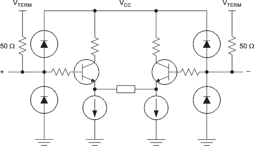 Figure 21. DisplayPort Input Stage
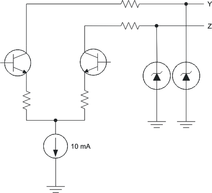 Figure 22. TMDS Output Stage
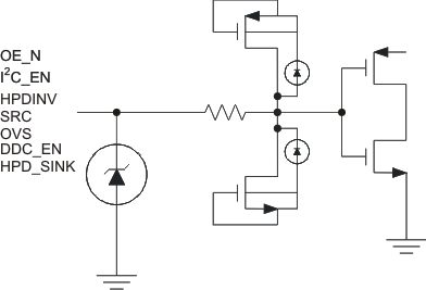 Figure 23. HPD and Control Input Stage
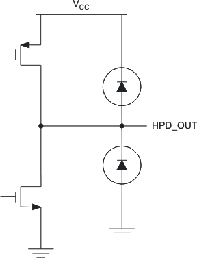 Figure 24. HPD Output Stage
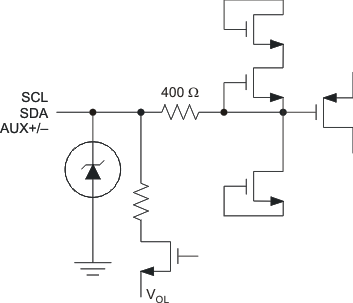 Figure 25. I2C Input and Output Stage
7.4 Device Functional Modes
7.4.1 Active
The SN75DP139 activates the main link channel and thus is able to transmit the TMDS content.
7.4.2 Low Power With DDC Channel Enabled
The SN75DP139 is in low power but keeps its DDC channel active, this allows the device to configure its internal I2C registers.
7.4.3 Low Power
The SN75DP139 is in the lowest power mode, with no activity on the DDC or main link channels.
7.5 Programming
7.5.1 I2C Interface Notes
The I2C interface can be used to access the internal memory of the SN75DP139. I2C is a two-wire serial interface developed by Philips Semiconductor (see I2C-Bus Specification, Version 2.1, January 2000). The bus consists of a data line (SDA) and a clock line (SCL) with pull-up structures. When the bus is idle, both SDA and SCL lines are pulled high. All the I2C compatible devices connect to the I2C bus through open drain I/O pins, SDA and SCL. A master device, usually a microcontroller or a digital signal processor, controls the bus. The master is responsible for generating the SCL signal and device addresses. The master also generates specific conditions that indicate the START and STOP of data transfer. A slave device receives and/or transmits data on the bus under control of the master device. The SN75DP139 works as a slave and supports the standard mode transfer (100 kbps) as defined in the I2C-Bus Specification.
The basic I2C start and stop access cycles are shown in Figure 26.
The basic access cycle consists of the following:
- A start condition
- A slave address cycle
- Any number of data cycles
- A stop condition
 Figure 26. I2C Start And Stop Conditions
7.5.2 General I2C Protocol
- The master initiates data transfer by generating a start condition. The start condition is when a high-to-low transition occurs on the SDA line while SCL is high, as shown in Figure 28. All I2C-compatible devices should recognize a start condition.
- The master then generates the SCL pulses and transmits the 7-bit address and the read/write direction bit R/W on the SDA line. During all transmissions, the master ensures that data is valid. A valid data condition requires the SDA line to be stable during the entire high period of the clock pulse (see Figure 27). All devices recognize the address sent by the master and compare it to their internal fixed addresses. Only the slave device with a matching address generates an acknowledge (see Figure 28) by pulling the SDA line low during the entire high period of the ninth SCL cycle. On detecting this acknowledge, the master knows that a communication link with a slave has been established.
- The master generates further SCL cycles to either transmit data to the slave (R/W bit 0) or receive data from the slave (R/W bit 1). In either case, the receiver needs to acknowledge the data sent by the transmitter. So an acknowledge signal can either be generated by the master or by the slave, depending on which one is the receiver. The 9-bit valid data sequences consisting of 8-bit data and 1-bit acknowledge can continue as long as necessary (See Figure 29).
- To signal the end of the data transfer, the master generates a stop condition by pulling the SDA line from low to high while the SCL line is high (see Figure 29). This releases the bus and stops the communication link with the addressed slave. All I2C compatible devices must recognize the stop condition. Upon the receipt of a stop condition, all devices know that the bus is released, and they wait for a start condition followed by a matching address.
 Figure 27. I2C Bit Transfer
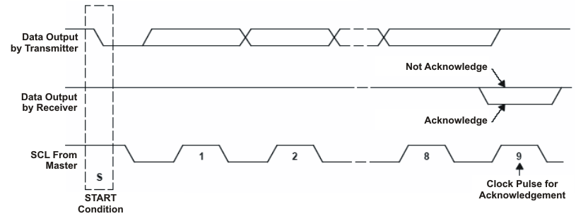 Figure 28. I2C Acknowledge
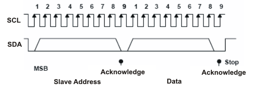 Figure 29. I2C Address And Data Cycles
During a read cycle, the slave receiver will acknowledge the initial address byte if it decodes the address as its address. Following this initial acknowledge by the slave, the master device becomes a receiver and acknowledges data bytes sent by the slave. When the master has received all of the requested data bytes from the slave, the not acknowledge (A) condition is initiated by the master by keeping the SDA signal high just before it asserts the stop (P) condition. This sequence terminates a read cycle as shown in Figure 30 and Figure 31. See Example – Reading from the SN75DP139 section for more information.
 Figure 30. I2C Read Cycle
 Figure 31. Multiple Byte Read Transfer
7.5.3 Slave Address
Both SDA and SCL must be connected to a positive supply voltage via a pull-up resistor. These resistors should comply with the I2C specification that ranges from 2kΩ to 19kΩ. When the bus is free, both lines are high. The address byte is the first byte received following the START condition from the master device. The 7-bit address is factory preset to 1000000. Table 3 lists the calls that the SN75DP139 will respond to.
Table 3. SN75DP139 Slave Address
| Fixed Address | Read/Write Bit | ||||||
|---|---|---|---|---|---|---|---|
| Bit 7 (MSB) |
Bit 6 | Bit 5 | Bit 4 | Bit 3 | Bit 2 | Bit 1 | Bit 0 (R/W) |
| 1 | 0 | 0 | 0 | 0 | 0 | 0 | 1 |
7.5.3.1 Sink Port Selection Register And Source Plug-In Status Register Description (Sub-Address)
The SN75DP139 operates using a multiple byte transfer protocol similar to Figure 31. The internal memory of the SN75DP139 contains the phrase “DP-HDMI ADAPTOR<EOT>” converted to ASCII characters. The internal memory address registers and the value of each can be found in Table 4.
During a read cycle, the SN75DP139 will send the data in its selected sub-address in a single transfer to the master device requesting the information. See the Example – Reading from the SN75DP139 section of this document for the proper procedure on reading from the SN75DP139.
Table 4. SN75DP139 Sink Port And Source Plug-In Status Registers Selection
| Address | 0x00 | 0x01 | 0x02 | 0x03 | 0x04 | 0x05 | 0x06 | 0x07 | 0x08 | 0x09 | 0x0A | 0x0B | 0x0C | 0x0D | 0x0E | 0x0F | 0x10 |
| Data | 44 | 50 | 2D | 48 | 44 | 4D | 49 | 20 | 41 | 44 | 41 | 50 | 54 | 4F | 52 | 04 | FF |
7.5.3.2 Example – Reading From The SN75DP139:
The read operation consists of several steps. The I2C master begins the communication with the transmission of the start sequence followed by the slave address of the SN75DP139 and logic address of 00h. The SN75DP139 will acknowledge it’s presence to the master and begin to transmit the contents of the memory registers. After each byte is transferred the SN75DP139 will wait for either an acknowledge (ACK) or a not-acknowledge (NACK) from the master. If an ACK is received the next byte of data will be transmitted. If a NACK is received the data transmission sequence is expected to end and the master should send the stop command.
The SN75DP139 will continue to send data as long as the master continues to acknowledge each byte transmission. If an ACK is received after the transmission of byte 0x0F the SN75DP139 will transmit byte 0x10 and continue to transmit byte 0x10 for all further ACK’s until a NACK is received.
The SN75DP139 also supports an accelerated read mode where steps 1–6 can be skipped.
SN75DP139 Read Phase
| Step 1 | 0 |
|---|---|
| I2C Start (Master) | S |
| Step 2 | 7 | 6 | 5 | 4 | 3 | 2 | 1 | 0 |
|---|---|---|---|---|---|---|---|---|
| I2C General Address Write (Master) | 1 | 0 | 0 | 0 | 0 | 0 | 0 | 0 |
| Step 3 | 9 |
|---|---|
| I2C Acknowledge (Slave) | A |
| Step 4 | 7 | 6 | 5 | 4 | 3 | 2 | 1 | 0 |
|---|---|---|---|---|---|---|---|---|
| I2C Logic Address (Master) | 0 | 0 | 0 | 0 | 0 | 0 | 0 | 0 |
| Step 5 | 9 |
|---|---|
| I2C Acknowledge (Slave) | A |
| Step 6 | 0 |
|---|---|
| I2C Stop (Master) | P |
| Step 7 | 0 |
|---|---|
| I2C Start (Master) | S |
| Step 8 | 7 | 6 | 5 | 4 | 3 | 2 | 1 | 0 |
|---|---|---|---|---|---|---|---|---|
| I2C General Address Read (Master) | 1 | 0 | 0 | 0 | 0 | 0 | 0 | 1 |
| Step 9 | 9 |
|---|---|
| I2C Acknowledge (Slave) | A |
| Step 10 | 7 | 6 | 5 | 4 | 3 | 2 | 1 | 0 |
|---|---|---|---|---|---|---|---|---|
| I2C Read Data (Slave) | Data | Data | Data | Data | Data | Data | Data | Data |
Where Data is determined by the Logic values Contained in the Sink Port Register
| Step 11 | 9 |
|---|---|
| I2C Not-Acknowledge (Master) | X |
Where X is an A (Acknowledge) or A (Not-Acknowledge)
An A causes the pointer to increment and step 10 is repeated.
An A causes the slave to stop transmitting and proceeds to step 12.
| Step 12 | 0 |
|---|---|
| I2C Stop (Master) | P |