SLLS846C May 2009 – August 2014 SN75LVDS83B
PRODUCTION DATA.
- 1 Features
- 2 Applications
- 3 Description
- 4 Revision History
- 5 Description (Continued)
- 6 Pin Configuration and Functions
- 7 Specifications
- 8 Parameter Measurement Information
- 9 Detailed Description
- 10Application and Implementation
- 11Power Supply Recommendations
- 12Layout
- 13Device and Documentation Support
- 14Mechanical, Packaging, and Orderable Information
8 Parameter Measurement Information
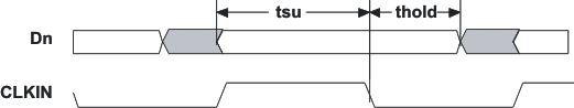
All input timing is defined at IOVDD / 2 on an input signal with a 10% to 90% rise or fall time of less than 3 ns. CLKSEL = 0 V.
Figure 6. Set Up and Hold Time Definition
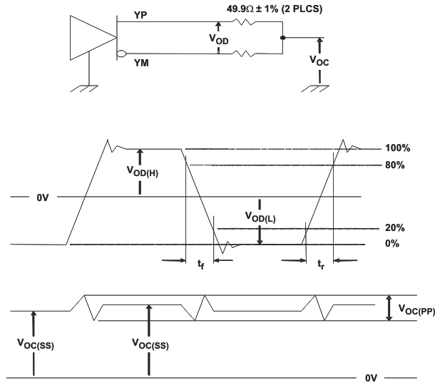 Figure 7. Test Load and Voltage Definitions for LVDS Outputs
The 16 grayscale test pattern test device power consumption for a typical display pattern.
Figure 8. 16 Grayscale Test Pattern
The worst-case test pattern produces nearly the maximum switching frequency for all of the LVDS outputs.
Figure 9. Worst-Case Power Test Pattern
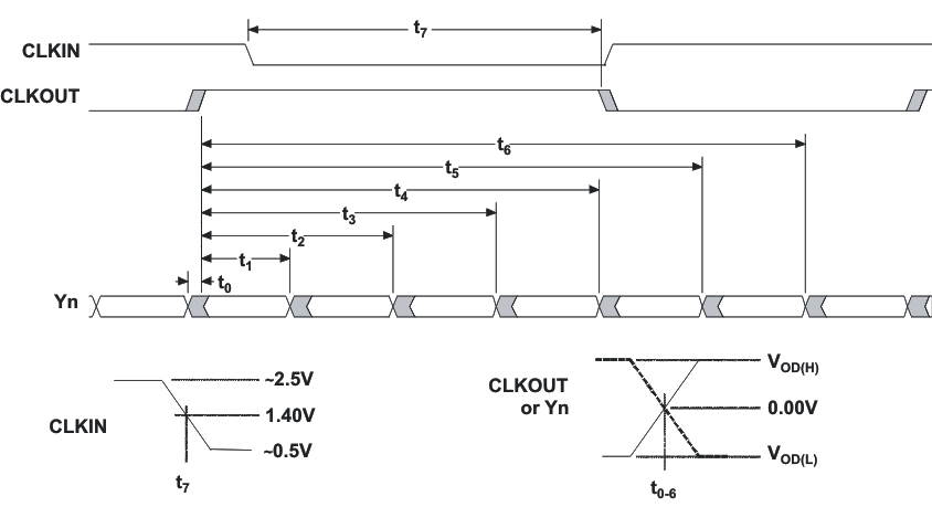
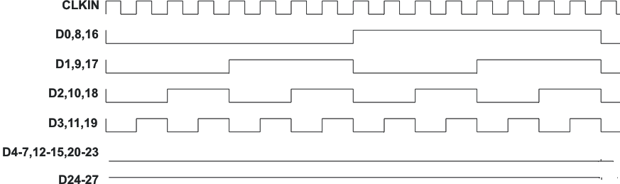
CLKOUT is shown with CLKSEL at high-level.
CLKIN polarity depends on CLKSEL input level.
Figure 10. SN75LVDS83B Timing Definitions
CLKIN polarity depends on CLKSEL input level.
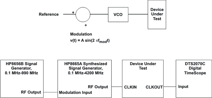 Figure 11. Output Clock Jitter Test Set Up
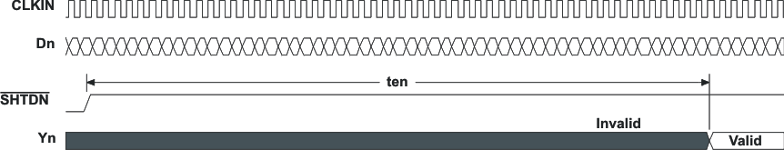 Figure 12. Enable Time Waveforms
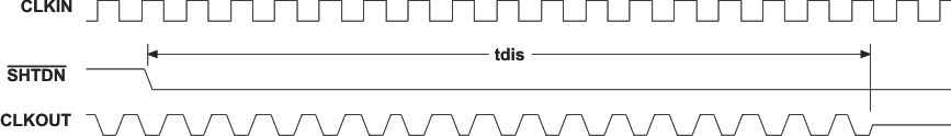 Figure 13. Disable Time Waveforms