SNAS670 July 2015 TDC1011-Q1
PRODUCTION DATA.
- 1 Features
- 2 Applications
- 3 Description
- 4 Revision History
- 5 Pin Configuration and Functions
- 6 Specifications
- 7 Parameter Measurement Information
-
8 Detailed Description
- 8.1 Overview
- 8.2 Functional Block Diagram
- 8.3 Feature Description
- 8.4 Device Function Description
- 8.5 Programming
- 8.6
Register Maps
- 8.6.1
TDC1011 Registers
- 8.6.1.1 CONFIG_0 Register (address = 0h) [reset = 45h]
- 8.6.1.2 CONFIG_1 Register (address = 1h) [reset = 40h]
- 8.6.1.3 CONFIG_2 Register (address = 2h) [reset = 0h]
- 8.6.1.4 CONFIG_3 Register (address 3h) [reset = 3h]
- 8.6.1.5 CONFIG_4 Register (address = 4h) [reset = 1Fh]
- 8.6.1.6 TOF_1 Register (address = 5h) [reset = 0h]
- 8.6.1.7 TOF_0 Register (address = 6h) [reset = 0h]
- 8.6.1.8 ERROR_FLAGS Register (address = 7h) [reset = 0h]
- 8.6.1.9 TIMEOUT Register (address = 8h) [reset = 19h]
- 8.6.1.10 CLOCK_RATE Register (address = 9h) [reset = 0h]
- 8.6.1
TDC1011 Registers
- 9 Application and Implementation
- 10Power Supply Recommendations
- 11Layout
- 12Device and Documentation Support
- 13Mechanical, Packaging, and Orderable Information
6 Specifications
6.1 Absolute Maximum Ratings
Over operating free-air temperature range (unless otherwise noted) (1)(2)| MIN | MAX | UNIT | ||
|---|---|---|---|---|
| VDD | Analog supply voltage, VDD pins | –0.3 | 6.0 | V |
| VIO | I/O supply voltage (VIO must always be lower than or equal to VDD supply) | –0.3 | 6.0 | V |
| VI | Voltage on any analog input pin(3) | –0.3 | VDD + 0.3 | V |
| VI | Voltage on any digital input pin(3) | –0.3 | VIO + 0.3 | V |
| II | Input current at any pin | 5 | mA | |
| TJ | Operating junction temperature | –40 | 125 | °C |
| Tstg | Storage temperature range | –65 | 150 | °C |
(1) Stresses beyond those listed under Absolute Maximum Ratings may cause permanent damage to the device. These are stress ratings only, which do not imply functional operation of the device at these or any other conditions beyond those indicated under Recommended Operating Conditions. Exposure to absolute-maximum-rated conditions for extended periods may affect device reliability.
(2) All voltages are with respect to ground, unless otherwise specified.
(3) When the input voltage at a pin exceeds the power supplies, the current at that pin must not exceed 5 mA and the voltage (VI) at that pin must not exceed 6.0 V.
6.2 ESD Ratings
| VALUE | UNIT | ||||
|---|---|---|---|---|---|
| V(ESD) | Electrostatic discharge | Human-body model (HBM), per AEC A100-002(1) | ±2000 | V | |
| Charged-device model (CDM), per AEC Q100-011 | All pins | ±500 | |||
| Corner pins (1, 14, 15 and 28) | ±750 | ||||
(1) AEC Q100-002 indicates HBM stressing is done in accordance with the ANSI/ESDA/JEDEC JS-001 specification.
6.3 Recommended Operating Conditions
Over operating free-air temperature range (unless otherwise noted)| MIN | MAX | UNIT | ||
|---|---|---|---|---|
| VDD | Analog supply voltage, VDD pins | 2.7 | 5.5 | V |
| VIO | Digital supply voltage, (VIO must always be lower than or equal to VDD supply) | 1.8 | VDD | V |
| VI | Voltage on any analog input pin | GND | VDD | V |
| VI | Voltage on any digital input pin | GND | VIO | V |
| ƒCLKIN | Operating frequency | 0.06 | 16 | MHz |
| TJ | Operating junction temperature | –40 | 125 | °C |
6.4 Thermal Information(1)
| THERMAL METRIC | TDC1011 TSSOP PW (28 PINS) |
UNIT | |
|---|---|---|---|
| RθJA | Junction-to-ambient thermal resistance | 83.5 | °C/W |
| RθJC(top) | Junction-to-case (top) thermal resistance | 29.9 | |
| RθJB | Junction-to-board thermal resistance | 40.8 | |
| ψJT | Junction-to-top characterization parameter | 2.4 | |
| ψJB | Junction-to-board characterization parameter | 40.3 | |
(1) For more information about traditional and new thermal metrics, see the IC Package Thermal Metrics application report, SPRA953.
6.5 Electrical Characteristics
The electrical ratings specified in this section apply to all specifications in this document, unless otherwise noted. These specifications are interpreted as conditions that do not degrade the device parametric or functional specifications for the life of the product containing it. TA = 25°C, VDD = VIO = 3.7 V, VCOM = VCM = VDD / 2, CVCOM = 10 nF (unless otherwise noted).| PARAMETER | TEST CONDITIONS | MIN | TYP | MAX | UNIT | ||
|---|---|---|---|---|---|---|---|
| TRANSMITTER SIGNAL PATH (TX) | |||||||
| VOUT(TX) | Output voltage swing | ƒout = 1 MHz, RL = 75 Ω to VCM | HIGH | VDD – 0.32 | V | ||
| LOW | 0.32 | V | |||||
| IOUT(TX) | Output drive current | ƒout = 1 MHz, RL = 75 Ω to VCM | 22 | mARMS | |||
| ƒOUT(TX) | Output TX frequency | ƒCLKIN = 8 MHz, divide-by-2 (programmable; see Transmitter Signal Path) | 4 | MHz | |||
| RECEIVER SIGNAL PATH (RX) | |||||||
| ΔtSTOP | STOP cycle-to-cycle jitter | LNA capacitive feedback, GPGA = 6 dB, ƒIN = 1 MHz, VIN = 100 mVPP, CVCOM = 1 µF and Figure 14 | 50 | psRMS | |||
| LNA | |||||||
| GLNA | LNA gain | Capacitive feedback, CIN = 300 pF, ƒIN = 1 MHz, RL = 100 kΩ to VCM, CVCOM = 1 µF | 20 | dB | |||
| enLNA | LNA input referred noise density | Capacitive feedback, CIN = 300 pF, ƒ = 1 MHz, VDD = 3.1 V, VIN = VCM, RL = ∞, CVCOM = 1 µF | 2 | nV/√Hz | |||
| VIN(LNA) | Input voltage range | Resistive feedback, RL = 1 kΩ to VCM, CVCOM = 1 µF | HIGH | VCM + (VCM – 0.24) / (GLNA) | V | ||
| LOW | VCM – (VCM – 0.24) / (GLNA) | V | |||||
| VOUT(LNA) | Output voltage range | Resistive feedback, RL = 1 kΩ to VCM, CVCOM = 1 µF | HIGH | VDD – 0.24 | V | ||
| LOW | GND + 0.24 | V | |||||
| SRLNA | Slew rate(6) | Resistive feedback, RL = 1 kΩ to VCM, 100mV step, CVCOM = 1 µF | 9 | V/μs | |||
| BWLNA | –3-dB bandwidth | Capacitive feedback, CIN = 300 pF, RL= 100 kΩ to VCM, CVCOM = 1 µF | 5 | MHz | |||
| VOS(LNA) | LNA input offset voltage | Resistive mode, VIN = VCM, RL = ∞ | ±320 | µV | |||
| VCOM | |||||||
| VCOM | VCOM output voltage | CVCOM = 1 µF | VCM | V | |||
| VCOM output error | 0.5% | ||||||
| PGA | |||||||
| VIN(PGA) | PGA input range | RL = 100 kΩ to VCM, CL = 10 pF to GND | HIGH | VCM + (VCM – 0.06) / (GPGA) | V | ||
| LOW | VCM – (VCM – 0.06) / (GPGA) | V | |||||
| GPGAMIN | PGA min gain | DC, RL = ∞, CL = 10 pF | 0 | dB | |||
| GPGAMAX | PGA max gain | 21 | dB | ||||
| ΔGPGA | PGA gain step size | 3 | dB | ||||
| GE(PGA) | PGA gain error | DC, GPGA = 0 dB, RL = ∞, CL = 10 pF | 5% | ||||
| TCGPGA | PGA gain temperature coefficient | DC, GPGA = 0 dB, RL = ∞, CL = 10 pF | 170 | ppm/°C | |||
| enPGA | PGA input referred noise density | GPGA = 21 dB, ƒ = 1 MHz, VDD = 3.1V, VIN = VCM, RL = ∞, CVCOM = 1 µF | 3.1 | nV/√Hz | |||
| VOUT(PGA) | Output range | RL = 100 kΩ to VCM, CL = 10 pF to GND | HIGH | VDD – 0.06 | V | ||
| LOW | 60 | mV | |||||
| BWPGA | –3-db bandwidth | GPGA = 21 dB, RL = 100 kΩ to VCM, CL = 10 pF, CVCOM = 1 µF | 5 | MHz | |||
| SRPGA | Slew rate(6) | GPGA = 21 dB, RL = 100 kΩ to VCM, CL = 10 pF, CVCOM = 1 µF | 12.5 | V/µs | |||
| ZERO CROSS COMPARATOR | |||||||
| VOS(COMP) | Input offset voltage(5) | Referred to VCOM | ±115 | µV | |||
| enCOMP | Zero crossing comparator input referred noise(5) | 1 MHz | 5 | nV/√Hz | |||
| HYSTCOMP | Hysteresis (5) | Referred to VCOM | -10 | mV | |||
| THRESHOLD DETECTOR | |||||||
| VTHDET | Threshold level | ECHO_QUAL_THLD = 0h, VCOM referred | –35 | mV | |||
| ECHO_QUAL_THLD = 7h, VCOM referred | –1.5 | V | |||||
| TEMPERATURE SENSOR INTERFACE(1) | |||||||
| TERROR | Temperature measurement accuracy | RREF = 1 kΩ, PT1000 range: –40 to 125°C(2) | 1 | °C | |||
| RREF = 1 kΩ, PT1000 range: –15°C to 85°C(2) | 0.5 | °C | |||||
| Relative accuracy | RREF = 1 kΩ, RRTD1 = RRTD2 = 1.1 kΩ | 0.02 | °CRMS | ||||
| TGE | Gain error | 5.8 | m°C/°C | ||||
| POWER SUPPLY | |||||||
| IDD | VDD supply current | Sleep (EN = CLKIN = TRIGGER = low) | 0.61 | µA | |||
| Continuous receive mode, LNA and PGA bypassed | 2.8 | 3 | mA | ||||
| Continuous receive mode, LNA and PGA active | 6.2 | 7.5 | mA | ||||
| Temp. measurement only (PT1000 mode)(3) | 370 | 400 | µA | ||||
| Temp. measurement (PT500 mode)(4) | 500 | 540 | µA | ||||
| IIO | VIO supply sleep current(5) | Sleep (EN = CLKIN = TRIGGER = low) | 2 | nA | |||
| DIGITAL INPUT/OUTPUT CHARACTERISTICS | |||||||
| VIL | Input logic low threshold | 0.2 × VIO | V | ||||
| VIH | Input logic high threshold | 0.8 × VIO | V | ||||
| VOL | Output logic low threshold | SDO pin, 100-μA current | 0.2 | V | |||
| SDO pin, 1.85-mA current | 0.4 | V | |||||
| START and STOP pins, 100-μA current | 0.5 | V | |||||
| START and STOP pins, 1.85-mA current | 0.6 | V | |||||
| ERRB pin, 100-μA current | 0.2 | V | |||||
| ERRB pin, 1.85-mA current | 0.4 | V | |||||
| VOH | Output logic high threshold | SDO pin, 100-μA current | VIO – 0.2 | V | |||
| SDO pin, 1.85-mA current | VIO – 0.6 | V | |||||
| START and STOP pins, 100-μA current | VIO – 0.5 | V | |||||
| START and STOP pins, 1.85-mA current | VIO – 0.6 | V | |||||
| ERRB pin, 0-µA current | VIO – 0.2 | V | |||||
| IOMAX | Maximum output current for SDO, START and STOP | 1.85 | mA | ||||
(1) With ideal external components. For more detail see Temp Sensor Measurement section.
(2) PT1000 RTD approximate resistance: 800 Ω ≡ –52°C, 931 Ω ≡ –18°C, 1.10 kΩ ≡ 26°C, 1.33 kΩ ≡ 86°C and 1.48 kΩ ≡ 125°C.
(3) Specified currents include 120μA which flows through the RTD sensor in PT1000 mode (TEMP_RTD_SEL = 0).
(4) Specified currents include 240μA which flows through the RTD sensor in PT500 mode (TEMP_RTD_SEL = 1).
(5) Specified by design.
(6) The slew rate is measured from 10% to 90% and is represented by the average of the rising and falling slew rates.
6.6 Timing Requirements
TA = 25°C, VDD = VIO = 3.7 V and ƒSCLK = 1 MHz (unless otherwise noted).| MIN | NOM | MAX | UNIT | ||
|---|---|---|---|---|---|
| ƒSCLK | Serial clock frequency | 26 | MHz | ||
| t1 | High period, SCLK | 16 | ns | ||
| t2 | Low period, SCLK | 16 | ns | ||
| t3 | Set-up time, nCS to SCLK | 10 | ns | ||
| t4 | Set-up time, SDI to SCLK | 12 | ns | ||
| t5 | Hold time, SCLK to SDI | 12 | ns | ||
| t6 | SCLK transition to SDO valid time | 16 | ns | ||
| t7 | Hold time, SCLK transition to nCS rising edge | 10 | ns | ||
| t8 | nCS inactive | 17 | ns | ||
| t9 | Hold time, SCLK transition to nCS falling edge | 10 | ns | ||
| tr / tf | Signal rise and fall times(1) | 1.8 | ns | ||
(1) The slew rate is measured from 10% to 90% and is represented by the average of the rising and falling slew rates.
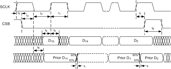 Figure 1. SPI Timing Diagram
6.7 Switching Characteristics
TA = 25°C, VDD = VIO = 3.7 V, ƒCLKIN = 8 MHz.| PARAMETER | TEST CONDITIONS | MIN | TYP | MAX | UNIT | |
|---|---|---|---|---|---|---|
| START, STOP, ENABLE, RESET, CLOCKIN, TRIGGER, ERR | ||||||
| PWSTART | Pulse width for START signal | TX_FREQ_DIV = 2h, NUM_TX = 1 | 1 | μs | ||
| TX_FREQ_DIV = 2h, NUM_TX = 2 | 2 | μs | ||||
| TX_FREQ_DIV = 2h, NUM_TX ≥ 3 | 3 | μs | ||||
| tr / tf START | Rise/fall time for START signal | 20% to 80%, 20-pF load | 0.25 | ns | ||
| tr / tf STOP | Rise/fall time for STOP signal | 20% to 80%, 20-pF load | 0.25 | ns | ||
| ƒCLKIN | Maximum CLKIN input frequency | 16 | MHz | |||
| tr / tf CLKIN | CLKIN input rise/fall time(1) | 20% to 80% | 10 | ns | ||
| tr / tf TRIG | TRIGGER input rise/fall time(1) | 20% to 80% | 10 | ns | ||
| tEN_TRIG | Enable to trigger wait time(1) | 50 | ns | |||
| tRES_TRIG | Reset to trigger wait time(1) | TX_FREQ_DIV = 2h (see TX/RX Measurement Sequencing and Timing) | 3.05 | μs | ||
(1) Specified by design.
6.8 Typical Characteristics
At TA = 25°C, unless otherwise noted.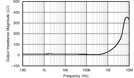
| VDD = VIO = 3.7V | Capacitive Feedback Mode | RL = 1kΩ |
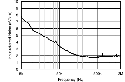
| VDD = VIO = 3.1V | Capacitive Feedback Mode | RL = ∞ |
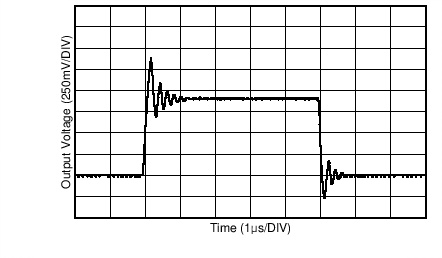
| VDD = VIO = 3.7V | Resistive Feedback Mode | RL = 1kΩ |
| VIN = 100mV | fIN = 100kHz | |
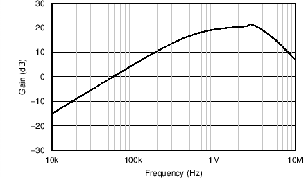
| VDD = VIO = 3.7V | Capacitive Feedback Mode | RL = 100kΩ |
| CIN = 300 pF |
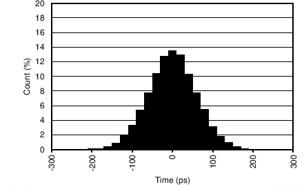
| VDD = VIO = 5V | LNA Capacitive Feedback Mode | PGA Gain of 6dB |
| VIN = 100mV | fIN = 1MHz | |
| (See Figure 14) | Count >= 10000 |

| VDD = VIO = 3.7V | LNA Capacitive Feedback Mode | PGA Gain of 6dB |
| VIN = 100mV | fIN = 1MHz | |
| TA = -40C° | (See Figure 14) | Count >= 10000 |
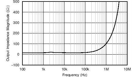
| VDD = VIO = 3.7V | Gain of 21dB | RL = 1kΩ |
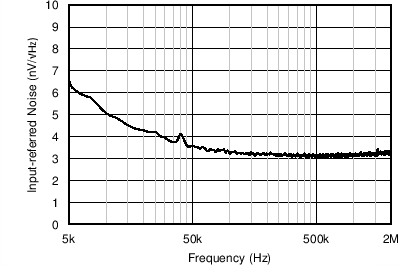
| VDD = VIO = 3.7V | Gain of 21dB | RL = ∞ |
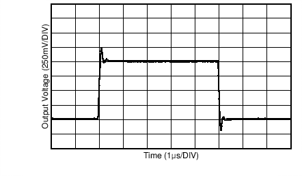
| VDD = VIO = 3.7V | Gain of 21dB | RL = 100kΩ |
| VIN = 100mV | fIN = 100kHz | |
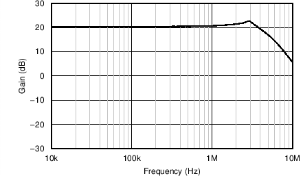
| VDD = VIO = 3.7V | Gain of 21dB | RL = 100kΩ |

| VDD = VIO = 3.7V | LNA Capacitive Feedback Mode | PGA Gain of 6dB |
| VIN = 100mV | fIN = 1MHz | |
| TA = 25C° | (See Figure 14) | Count >= 10000 |
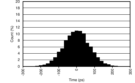
| VDD = VIO = 3.7V | LNA Capacitive Feedback Mode | PGA Gain of 6dB |
| VIN = 100mV | fIN = 1MHz | |
| TA = 125C° | (See Figure 14) | Count >= 10000 |