JAJSDS8C September 2017 – May 2019 TDP142
PRODUCTION DATA.
- 1 特長
- 2 アプリケーション
- 3 概要
- 4 改訂履歴
- 5 Pin Configuration and Functions
- 6 Specifications
- 7 Parameter Measurement Information
-
8 Detailed Description
- 8.1 Overview
- 8.2 Functional Block Diagram
- 8.3 Feature Description
- 8.4 Device Functional Modes
- 8.5 Programming
- 8.6
Register Maps
- 8.6.1 General Register (address = 0x0A) [reset = 00000001]
- 8.6.2 DisplayPort Control/Status Registers (address = 0x10) [reset = 00000000]
- 8.6.3 DisplayPort Control/Status Registers (address = 0x11) [reset = 00000000]
- 8.6.4 DisplayPort Control/Status Registers (address = 0x12) [reset = 00000000]
- 8.6.5 DisplayPort Control/Status Registers (address = 0x13) [reset = 00000000]
- 9 Application and Implementation
- 10Power Supply Recommendations
- 11Layout
- 12デバイスおよびドキュメントのサポート
- 13メカニカル、パッケージ、および注文情報
11.2 Layout Example
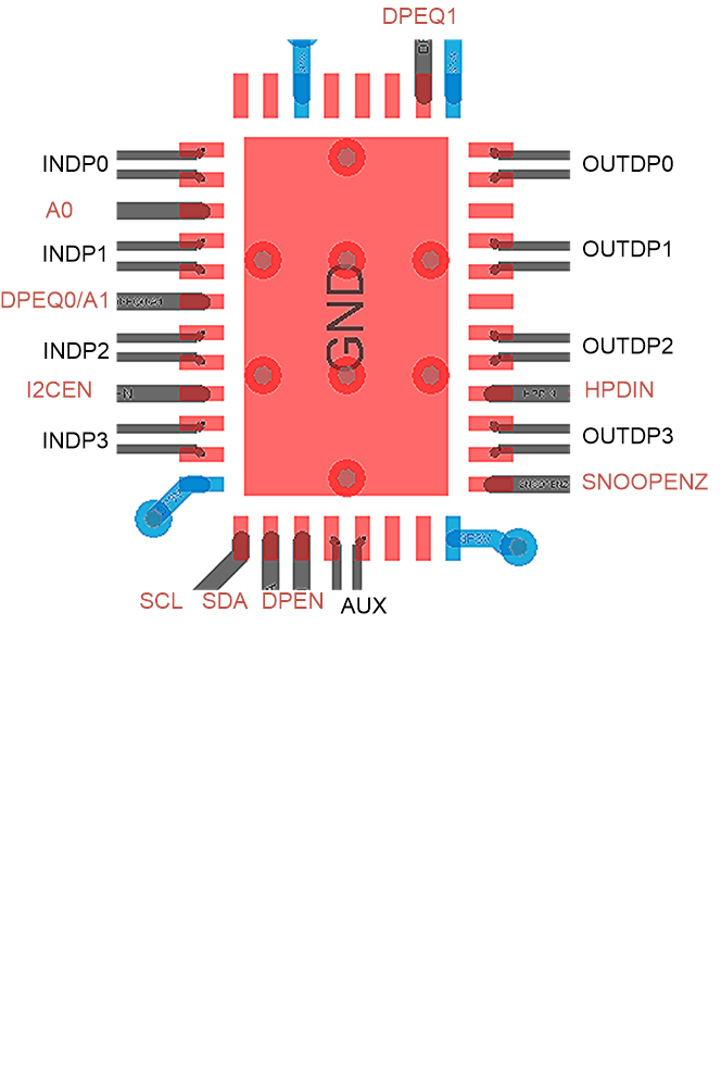
 Figure 21. Layout Example
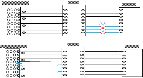
 Figure 22 demonstrates the solution of mismatched order between the output of the device and the DisplayPort connector for the source using BGA package. Top image of Figure 22 shows the crossing section between TDP142 and connector. Usually, Vias would be applied to avoid the cross, but using Via can attenuate the signal integrity. Therefore, the polarity swap would be implemented at the input of TDP142. The bottom image shows there is no more crossing section between the TDP142 and connector, which can minimize the number of Vias being used. Note that, the solution is only useful for the source using BGA package.
 Figure 22. Layout Example, Top: signal crossing on the output. Bottom: INDP2 and INDP3 Polarity Swap