SLOS829A February   2013  – July 2015 THS4532

PRODUCTION DATA.  

  1. Features
  2. Applications
  3. Description
  4. Revision History
  5. Related Products
  6. Pin Configuration and Functions
  7. Specifications
    1. 7.1 Absolute Maximum Ratings
    2. 7.2 ESD Ratings
    3. 7.3 Recommended Operating Conditions
    4. 7.4 Thermal Information
    5. 7.5 Electrical Characteristics: VS = 2.7 V
    6. 7.6 Electrical Characteristics: VS = 5 V
    7. 7.7 Typical Characteristics
      1. 7.7.1 Typical Characteristics: VS = 2.7 V
      2. 7.7.2 Typical Characteristics: VS = 5 V
  8. Detailed Description
    1. 8.1 Overview
    2. 8.2 Functional Block Diagram
    3. 8.3 Feature Description
      1. 8.3.1 Input Common-Mode Voltage Range
        1. 8.3.1.1 Setting the Output Common-Mode Voltage
      2. 8.3.2 Power Down
    4. 8.4 Device Functional Modes
  9. Application and Implementation
    1. 9.1 Application Information
      1. 9.1.1  Frequency Response and Output Impedance
      2. 9.1.2  Distortion
      3. 9.1.3  Slew Rate, Transient Response, Settling Time, Overdrive, Output Voltage, and Turnon and Turnoff Time
      4. 9.1.4  Common-Mode and Power Supply Rejection
      5. 9.1.5  VOCM Input
      6. 9.1.6  Balance Error
      7. 9.1.7  Single-Supply Operation
      8. 9.1.8  Low-Power Applications and the Effects of Resistor Values on Bandwidth
      9. 9.1.9  Driving Capacitive Loads
      10. 9.1.10 Audio Performance
      11. 9.1.11 Audio On and Off Pop Performance
    2. 9.2 Typical Applications
      1. 9.2.1 SAR ADC Performance: THS5432 and ADS8321 Combined Performance
        1. 9.2.1.1 Design Requirements
        2. 9.2.1.2 Detailed Design Procedure
        3. 9.2.1.3 Application Curve
      2. 9.2.2 Audio ADC Driver Performance: THS5432 and PCM4204 Combined Performance
        1. 9.2.2.1 Design Requirements
        2. 9.2.2.2 Detailed Design Procedure
        3. 9.2.2.3 Application Curves
      3. 9.2.3 SAR ADC Performance: THS5432 and ADS7945 Combined Performance
        1. 9.2.3.1 Design Requirements
        2. 9.2.3.2 Detailed Design Procedure
        3. 9.2.3.3 Application Curve
    3. 9.3 Systems Examples
      1. 9.3.1 Differential-Input to Differential-Output Amplifier
        1. 9.3.1.1 AC-Coupled, Differential-Input to Differential-Output Design Issues
      2. 9.3.2 Single-Ended to Differential FDA Configuration
        1. 9.3.2.1 Input Impedance
      3. 9.3.3 Single-Ended Input to Differential Output Amplifier
        1. 9.3.3.1 AC-Coupled Signal Path Considerations for Single-Ended Input to Differential Output Conversion
        2. 9.3.3.2 DC-Coupled Input Signal Path Considerations for Single-Ended to Differential Conversion
        3. 9.3.3.3 Resistor Design Equations for the Single-Ended to Differential Configuration of the FDA
      4. 9.3.4 Differential Input to Single-Ended Output Amplifier
  10. 10Power Supply Recommendations
  11. 11Layout
    1. 11.1 Layout Guidelines
    2. 11.2 Layout Example
  12. 12Device and Documentation Support
    1. 12.1 Documentation Support
    2. 12.2 Community Resources
    3. 12.3 Trademarks
    4. 12.4 Electrostatic Discharge Caution
    5. 12.5 Glossary
  13. 13Mechanical, Packaging, and Orderable Information

パッケージ・オプション

メカニカル・データ(パッケージ|ピン)
サーマルパッド・メカニカル・データ
発注情報

6 Pin Configuration and Functions

PW Package
16-Pin TSSOP
Top View
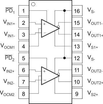
THS4532 po_los829.gif

Pin Functions

PIN I/O DESCRIPTION
NAME NO.
PD1 1 Power-down 1, PD = logic low = low power mode, PD = logic high = normal operation
(PIN MUST BE DRIVEN)
PD2 5 Amplifier 2 Power-down, PD = logic low = low power mode, PD = logic high = normal operation
(PIN MUST BE DRIVEN)
VIN1+ 2 I Noninverting amplifier 1 input
VIN1- 3 I Inverting amplifier 1 input
VIN2+ 6 I Noninverting amplifier 2 input
VIN2- 7 I Inverting amplifier 2 input
VOCM1 4 I Common-mode voltage input 1
VOCM2 8 I Common-mode voltage input 2
VOUT1+ 14 O Noninverting amplifier 1 output
VOUT1- 15 O Inverting amplifier 1 output
VOUT2+ 10 O Noninverting amplifier 2 output
VOUT2- 11 O Inverting amplifier 2 output
VS- 12, 16 I Negative power-supply input. Note VS– tied together on multichannel devices
VS1+ 13 I Amplifier 1 positive power-supply input
VS2+ 9 I Amplifier 2 positive power-supply input