SLVS719G June 2008 – January 2015 TL1963A
PRODUCTION DATA.
- 1 Features
- 2 Applications
- 3 Description
- 4 Revision History
- 5 Description (continued)
- 6 Device Comparison Table
- 7 Pin Configuration and Functions
- 8 Specifications
- 9 Detailed Description
- 10Application and Implementation
- 11Power Supply Recommendations
- 12Layout
- 13Device and Documentation Support
- 14Mechanical, Packaging, and Orderable Information
パッケージ・オプション
メカニカル・データ(パッケージ|ピン)
サーマルパッド・メカニカル・データ
発注情報
8 Specifications
8.1 Absolute Maximum Ratings
over operating virtual-junction temperature range (unless otherwise noted) (1)| MIN | MAX | UNIT | ||
|---|---|---|---|---|
| Input voltage, VIN | IN | –20 | 20 | V |
| OUT | –20 | 20 | ||
| Input-to-output differential(2) | –20 | 20 | ||
| SENSE | –20 | 20 | ||
| ADJ | –7 | 7 | ||
| SHDN | –20 | 20 | ||
| Output short-circuit duration, tshort | Indefinite | |||
| Maximum lead temperature (10-s soldering time), Tlead | 300 | °C | ||
| Maximum junction temperature, TJMAX | 125 | °C | ||
| Storage temperature, Tstg | –65 | 150 | °C | |
(1) Stresses beyond those listed under Absolute Maximum Ratings may cause permanent damage to the device. These are stress ratings only, and functional operation of the device at these or any other conditions beyond those indicated under Recommended Operating Conditions is not implied. Exposure to conditions beyond the recommended operating maximum for extended periods may affect device reliability.
(2) Absolute maximum input-to-output differential voltage cannot be achieved with all combinations of rated IN pin and OUT pin voltages. With the IN pin at 20 V, the OUT pin may not be pulled below 0 V. The total measured voltage from IN to OUT can not exceed ±20 V.
8.2 ESD Ratings
| VALUE | UNIT | |||
|---|---|---|---|---|
| V(ESD) | Electrostatic discharge | Human body model (HBM), per ANSI/ESDA/JEDEC JS-001(1) | ±2000 | V |
| Charged-device model (CDM), per JEDEC specification JESD22-C101(2) | ±1000 | |||
(1) JEDEC document JEP155 states that 500-V HBM allows safe manufacturing with a standard ESD control process.
(2) JEDEC document JEP157 states that 250-V CDM allows safe manufacturing with a standard ESD control process.
8.3 Recommended Operating Conditions
over operating free-air temperature range (unless otherwise noted)| MIN | MAX | UNIT | |||
|---|---|---|---|---|---|
| VIN | Input voltage range(1) | VOUT + VDO | 20 | V | |
| VIH | SHDN High-Level Input Voltage | 2 | 20 | V | |
| VIL | SHDN Low-Level Input Voltage | 0.25 | V | ||
| TJ | Recommended operating junction temperature range | –40 | 125 | °C | |
(1) TL1963A, TL1963A-15, and TL1963A-18 may require a higher minimum input voltage under some output voltage/load conditions as indicated under Electrical Characteristics.
8.4 Thermal Information
| THERMAL METRIC(1)(2) | TL1963A-xx | UNIT | |||
|---|---|---|---|---|---|
| KTT | DCQ | DCY | |||
| 5 PINS | 6 PINS | 4 PINS | |||
| RθJA | Junction-to-ambient thermal resistance | 32.9 | 50.5 | 57.9 | °C/W |
| RθJC(top) | Junction-to-case (top) thermal resistance | 37.6 | 31.1 | 38.6 | |
| RθJB | Junction-to-board thermal resistance | 18.9 | 5.1 | 7.1 | |
| ψJT | Junction-to-top characterization parameter | 5.7 | 1.0 | 1.7 | |
| ψJB | Junction-to-board characterization parameter | 17.3 | 5.0 | 7.0 | |
| RθJC(bot) | Junction-to-case (bottom) thermal resistance | 1.0 | — | — | |
(1) For more information about traditional and new thermal metrics, see the IC Package Thermal Metrics application report, SPRA953.
(2) For thermal estimates of this device based on PCB copper area, see the TI PCB Thermal Calculator.
8.5 Electrical Characteristics
Over recommended operating temperature range TJ = –40 to 125 °C (unless otherwise noted)(1)| PARAMETER | TEST CONDITIONS | TJ | MIN | TYP(10) | MAX | UNIT | ||
|---|---|---|---|---|---|---|---|---|
| VIN | Minimum input voltage(2)(3) | ILOAD = 0.5 A | 25°C | 1.9 | V | |||
| ILOAD = 1.5 A | Full range | 2.1 | 2.5 | |||||
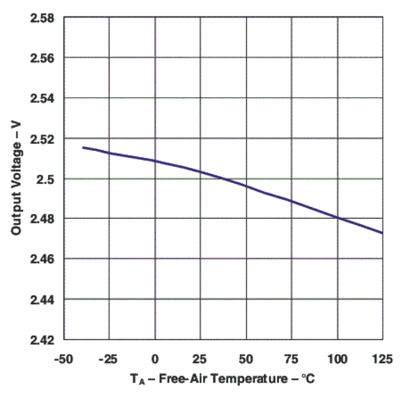
| VOUT | Regulated output voltage(4) | TL1963A-15 | VIN = 2.21 V, ILOAD = 1 mA | 25°C | 1.477 | 1.5 | 1.523 | V |
| VIN = 2.5 V to 20 V, ILOAD = 1 mA to 1.5 A |
Full range | 1.447 | 1.5 | 1.545 | ||||
| TL1963A-18 | VIN = 2.3 V, ILOAD = 1 mA | 25°C | 1.773 | 1.8 | 1.827 | |||
| VIN = 2.8 V to 20 V, ILOAD = 1 mA to 1.5 A |
Full range | 1.737 | 1.8 | 1.854 | ||||
| TL1963A-25 | VIN = 3 V, ILOAD = 1 mA | 25°C | 2.462 | 2.5 | 2.538 | |||
| VIN = 3.5 V to 20 V, ILOAD = 1 mA to 1.5 A |
Full range | 2.412 | 2.5 | 2.575 | ||||
| TL1963A-33 | VIN = 3.8 V, ILOAD = 1 mA | 25°C | 3.25 | 3.3 | 3.35 | |||
| VIN = 4.3 V to 20 V, ILOAD = 1 mA to 1.5 A |
Full range | 3.2 | 3.3 | 3.4 | ||||
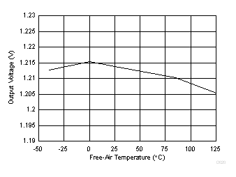
| VADJ | ADJ pin voltage(2)(4) | TL1963A | VIN = 2.21 V, ILOAD = 1 mA | 25°C | 1.192 | 1.21 | 1.228 | V |
| VIN = 2.5 V to 20 V, ILOAD = 1 mA to 1.5 A |
Full range | 1.174 | 1.21 | 1.246 | ||||
| Line regulation | TL1963A-15 | ΔVIN = 2.21 V to 20 V, ILOAD = 1 mA |
Full range | 2 | 6 | mV | ||
| TL1963A-18 | ΔVIN = 2.3 V to 20 V, ILOAD = 1 mA |
Full range | 2.5 | 7 | ||||
| TL1963A-25 | ΔVIN = 3 V to 20 V, ILOAD = 1 mA |
Full range | 3 | 10 | ||||
| TL1963A-33 | ΔVIN = 3.8 V to 20 V, ILOAD = 1 mA |
Full range | 3.5 | 10 | ||||
| TL1963A(2) | ΔVIN = 2.21 V to 20 V, ILOAD = 1 mA |
Full range | 1.5 | 5 | ||||
| Load regulation | TL1963A-15 | VIN = 2.5 V, ΔILOAD = 1 mA to 1.5 A |
25°C | 2 | 9 | mV | ||
| Full range | 18 | |||||||
| TL1963A-18 | VIN = 2.8 V, ΔILOAD = 1 mA to 1.5 A |
25°C | 2 | 10 | ||||
| Full range | 20 | |||||||
| TL1963A-25 | VIN = 3.5 V, ΔILOAD = 1 mA to 1.5 A |
25°C | 2.5 | 15 | ||||
| Full range | 30 | |||||||
| TL1963A-33 | VIN = 4.3 V, ΔILOAD = 1 mA to 1.5 A |
25°C | 3 | 20 | ||||
| Full range | 70 | |||||||
| TL1963A(2) | VIN = 2.5 V, ΔILOAD = 1 mA to 1.5 A |
25°C | 2 | 8 | ||||
| Full range | 18 | |||||||
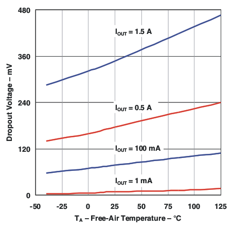
| VDO | Dropout voltage(3)(6)(5)
VIN = VOUT(NOMINAL) |
ILOAD = 1 mA | 25°C | 0.02 | 0.06 | V | ||
| Full range | 0.1 | |||||||
| ILOAD = 100 mA | 25°C | 0.1 | 0.17 | |||||
| Full range | 0.22 | |||||||
| ILOAD = 500 mA | 25°C | 0.19 | 0.27 | |||||
| Full range | 0.35 | |||||||
| ILOAD = 1.5 A | 25°C | 0.34 | 0.45 | |||||
| Full range | 0.55 | |||||||
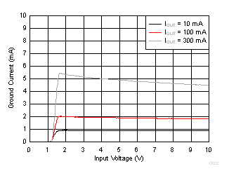
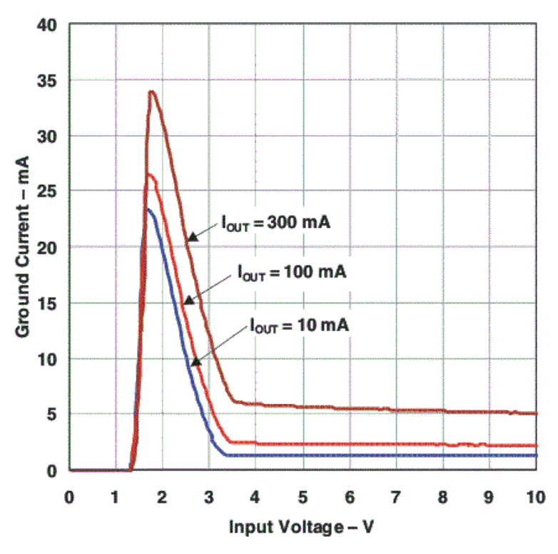
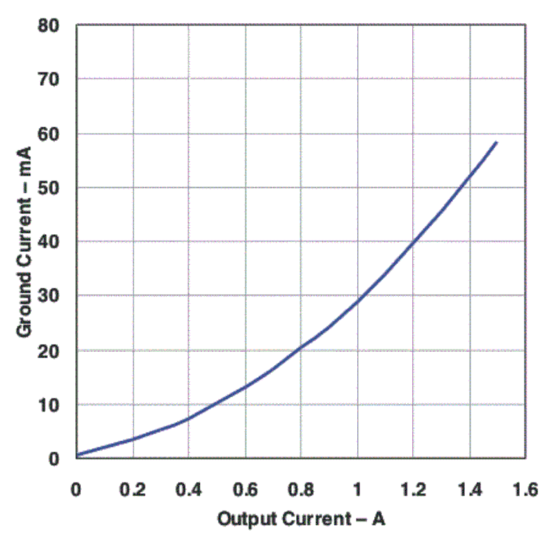
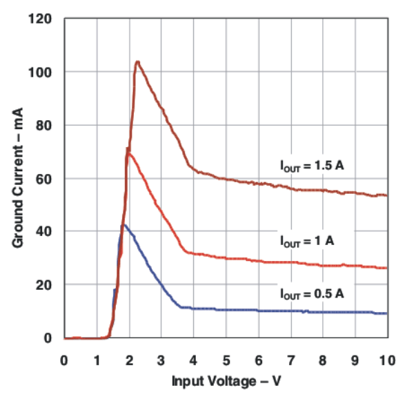
| IGND | GND pin current(5)(7)
VIN = VOUT(NOMINAL) + 1 |
ILOAD = 0 mA | Full range | 1 | 1.5 | mA | ||
| ILOAD = 1 mA | Full range | 1.1 | 1.6 | |||||
| ILOAD = 100 mA | Full range | 3.8 | 5.5 | |||||
| ILOAD = 500 mA | Full range | 15 | 25 | |||||
| ILOAD = 1.5 A | Full range | 80 | 120 | |||||
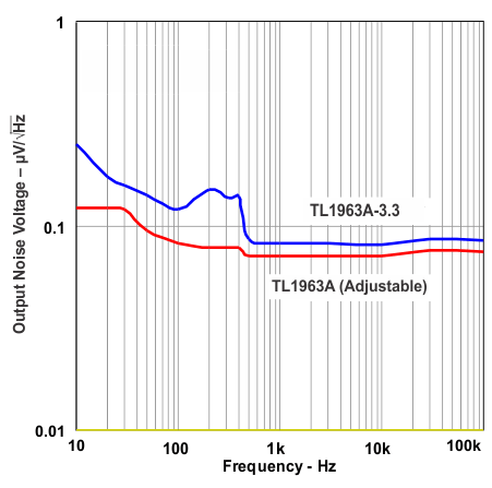
| eN | Output voltage noise | COUT = 10 μF, ILOAD = 1.5 A, BW = 10 Hz to 100 kHz |
25°C | 40 | μVRMS | |||
| IADJ | ADJ pin bias current(2)(8) | 25°C | 3 | 10 | μA | |||
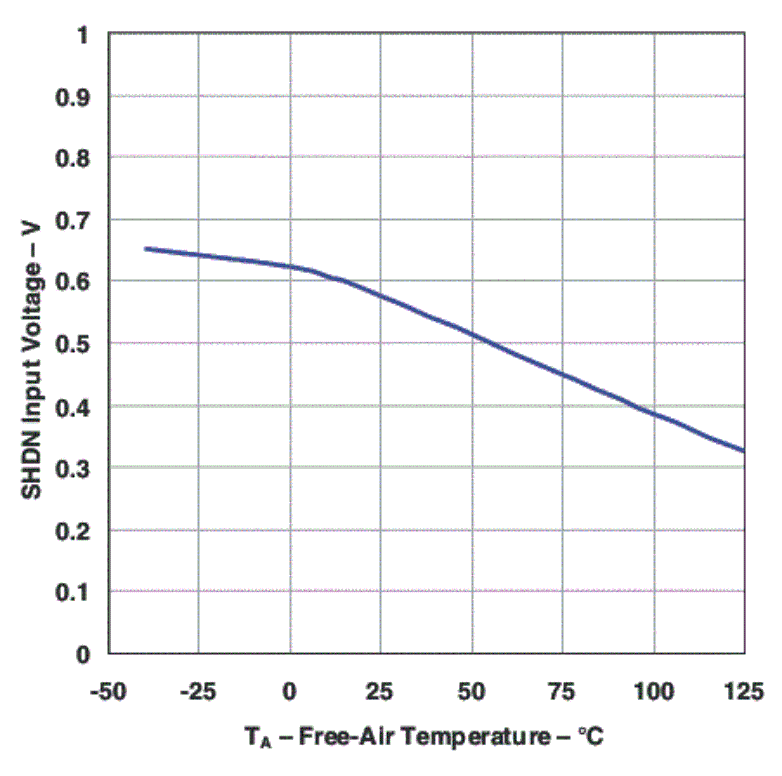
| Shutdown threshold | VOUT = OFF to ON | Full range | 0.9 | 2 | V | |||
| VOUT = ON to OFF | Full range | 0.25 | 0.75 | |||||
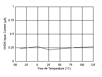
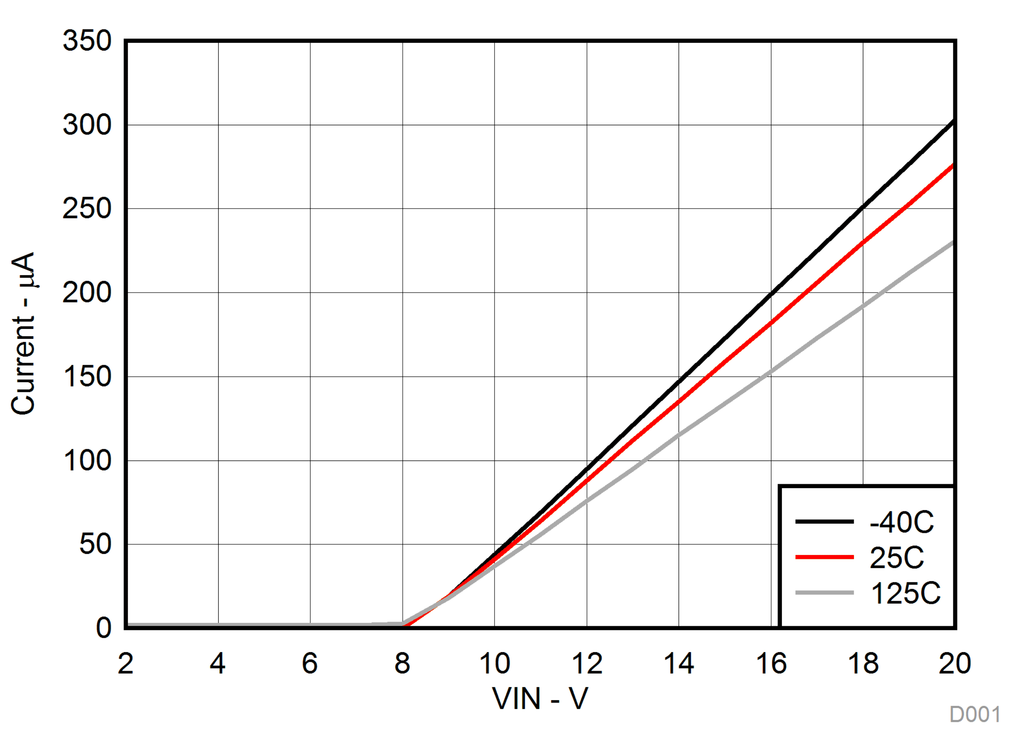
| ISHDN | SHDN pin current | VSHDN = 0 V | 25°C | 0.01 | 1 | μA | ||
| VSHDN = 20 V | 25°C | 3 | 30 | |||||
| Quiescent current in shutdown | VIN = 6 V, VSHDN = 0 V | 25°C | 0.01 | 1 | μA | |||
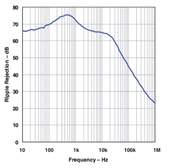
| Ripple rejection | VIN – VOUT = 1.5 V (avg), VRIPPLE = 0.5 VP-P, fRIPPLE = 120 Hz, ILOAD = 0.75 A |
25°C | 55 | 63 | dB | |||
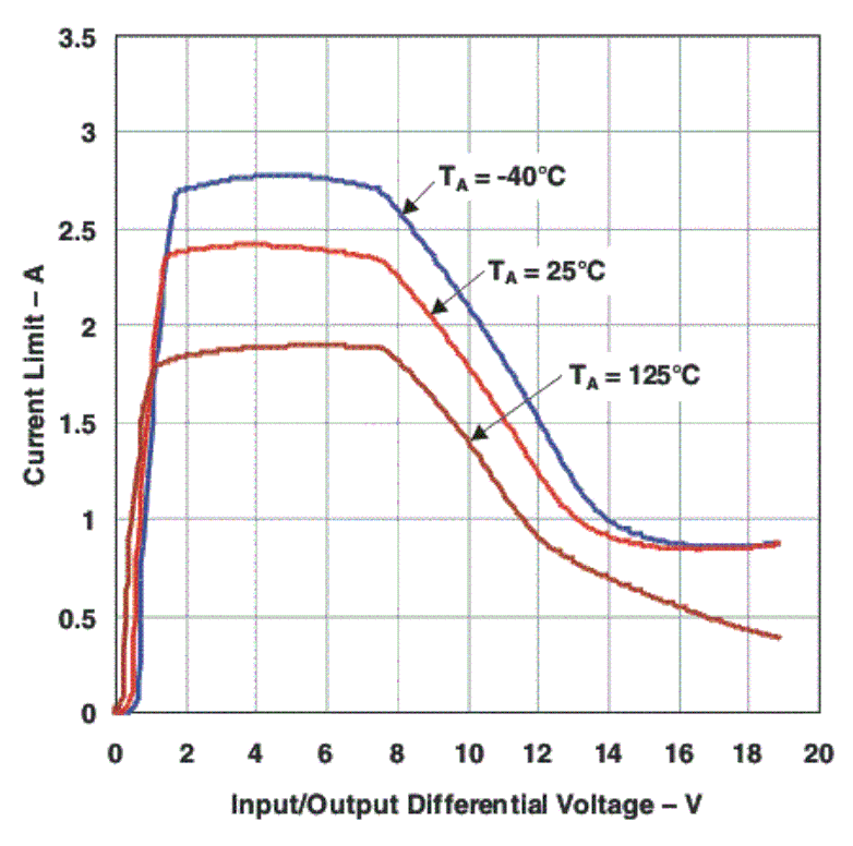
| ILIMIT | Current limit | VIN = 7 V, VOUT = 0 V | 25°C | 2 | A | |||
| VIN = VOUT(NOMINAL) + 1 | Full range | 1.6 | ||||||
| IIL | Input reverse leakage current | VIN = –20 V, VOUT = 0 V | Full range | 1 | μA | |||
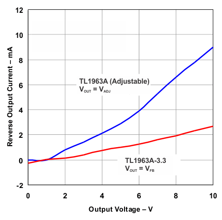
| IRO | Reverse output current(9) | TL1963A-15 | VOUT = 1.5 V, VIN < 1.5 V | 25°C | 600 | 1200 | μA | |
| TL1963A-18 | VOUT = 1.8 V, VIN < 1.8 V | 25°C | 600 | 1200 | ||||
| TL1963A-25 | VOUT = 2.5 V, VIN < 2.5 V | 25°C | 600 | 1200 | ||||
| TL1963A-33 | VOUT = 3.3 V, VIN < 3.3 V | 25°C | 600 | 1200 | ||||
| TL1963A | VOUT = 1.21 V, VIN < 1.21 V | 25°C | 300 | 600 | ||||
(1) The TL1963A-xx regulators are tested and specified under pulse load conditions such that TJ ≉ TA. They are fully tested at TA = 25°C. Performance at –40 and 125°C is specified by design, characterization, and correlation with statistical process controls.
(2) The TL1963A is tested and specified for these conditions with the ADJ pin connected to the OUT pin.
(3) For the TL1963A, TL1963A-15 and TL1963A-18, dropout voltages are limited by the minimum input voltage specification under some output voltage/load conditions.
(4) Operating conditions are limited by maximum junction temperature. The regulated output voltage specification does not apply for all possible combinations of input voltage and output current. When operating at maximum input voltage, the output current range must be limited. When operating at maximum output current, the input voltage range must be limited.
(5) To satisfy requirements for minimum input voltage, the TL1963A is tested and specified for these conditions with an external resistor divider (two 4.12-kΩ resistors) for an output voltage of 2.4 V. The external resistor divider adds a 300-µA DC load on the output.
(6) Dropout voltage is the minimum input to output voltage differential needed to maintain regulation at a specified output current. In dropout, the output voltage is equal to: VIN – VDROPOUT.
(7) GND pin current is tested with VIN = (VOUT(NOMINAL) + 1 V) and a current source load. The GND pin current decreases at higher input voltages.
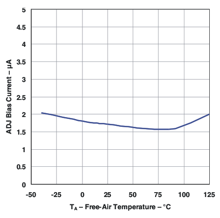
(8) ADJ pin bias current flows into the ADJ pin.
(9) Reverse output current is tested with the IN pin grounded and the OUT pin forced to the rated output voltage. This current flows into the OUT pin and out the GND pin.
(10) Typical values represent the likely parametric nominal values determined at the time of characterization. Typical values depend on the application and configuration and may vary over time. Typical values are not ensured on production material.
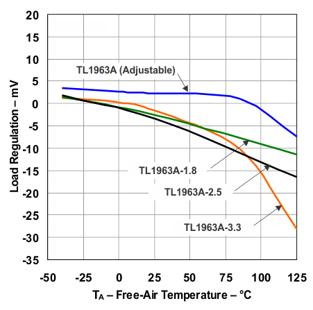
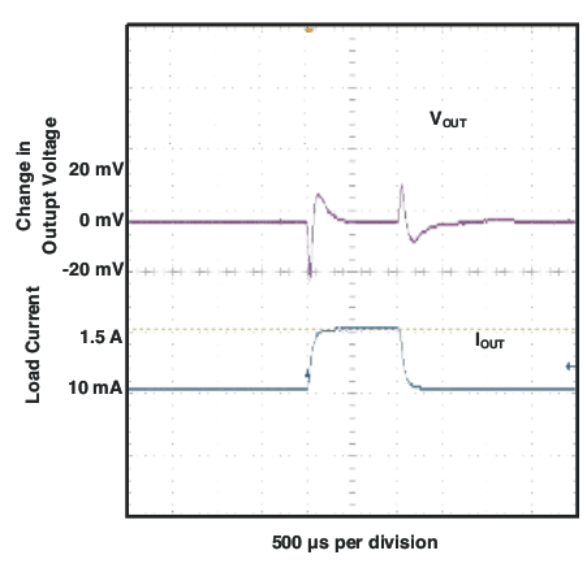
8.6 Typical Characteristics
Typical characteristics apply to all TL1963A-xx devices unless otherwise noted.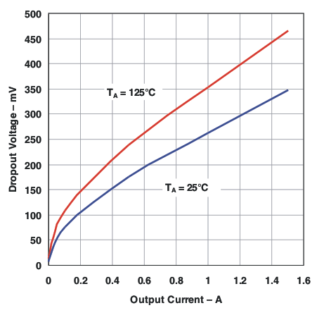
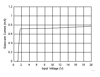
| VIN = 6 V | IOUT = 0 A | VSHDN = VIN |
| IOUT = 1 mA | TL1963A-25 |
| IOUT = 1 mA | VIN = 6 V |
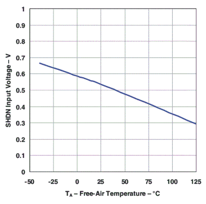
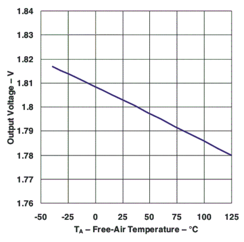
| TJ = 25 °C | VOUT = 1.21 V | VSHDN = VIN |
| TJ = 25 °C | VSHDN = VIN |
| VIN = VOUT(nom) + 1 | ||
| VSHON = 0 V |
| IOUT = 1 mA |
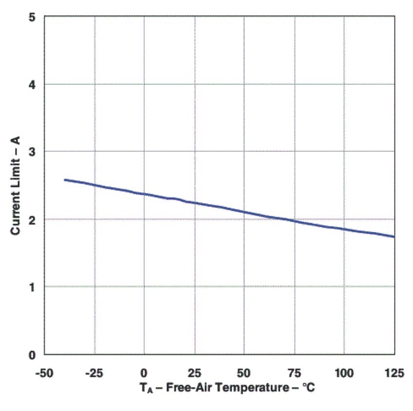
| VIN = 7 V | VOUT = 0 V |
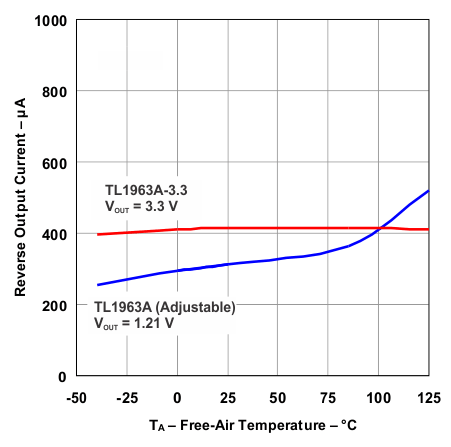
| VIN = 0 V |
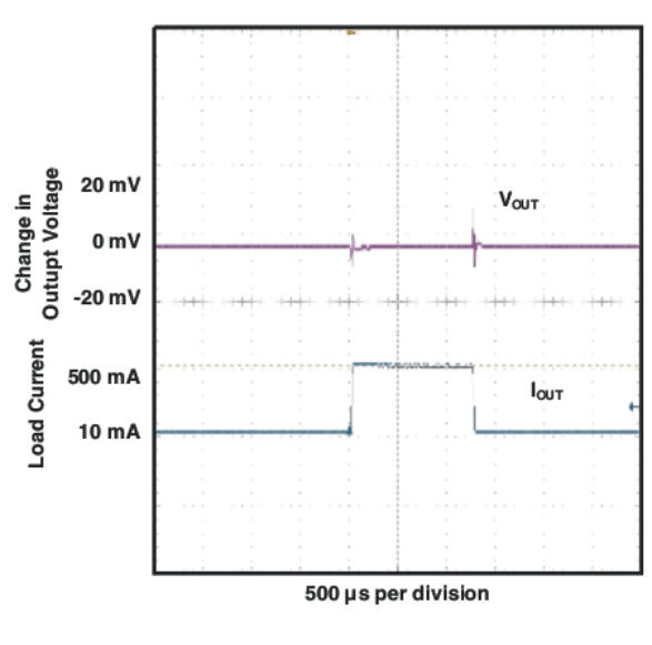
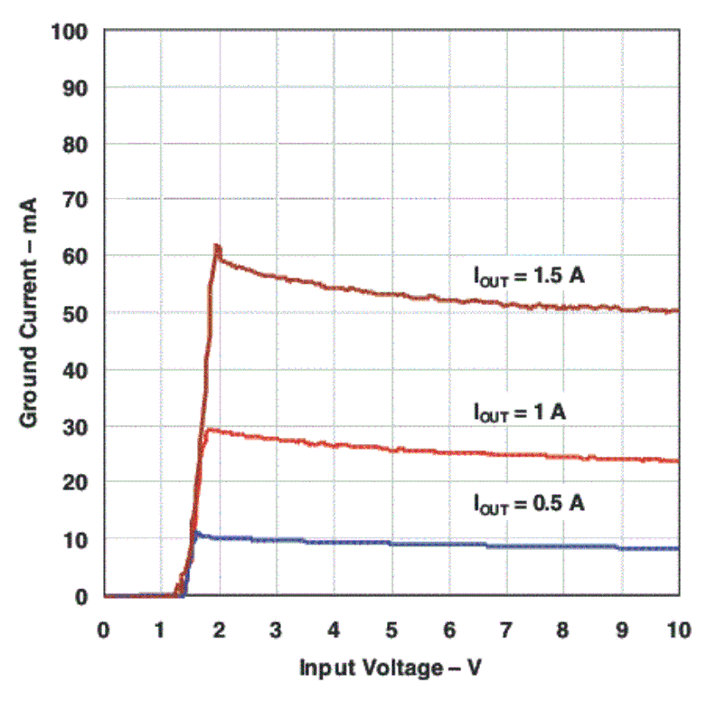
| IOUT = 1 mA to 1.5 A | ||
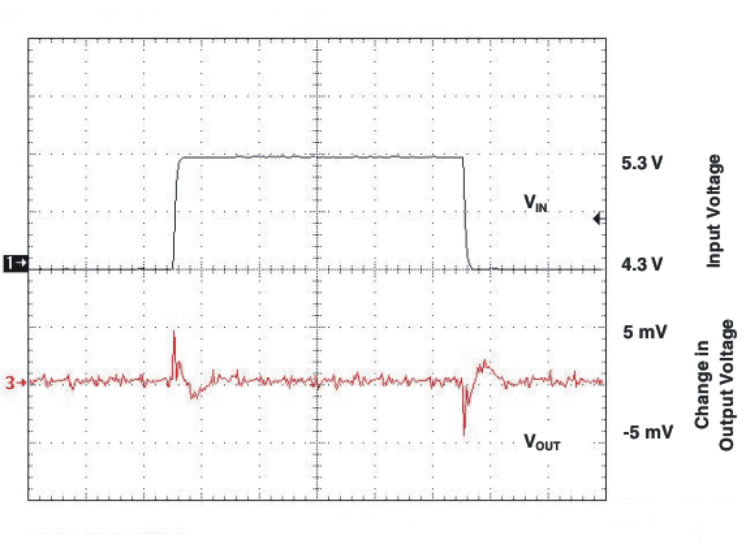
| VIN = 4.3 V | CIN = 10 µF | |
| COUT = 10 µF (ceramic) | ||
| IOUT = 1.5 A | CIN = 10 µF | |
| COUT = 10 µF (ceramic) | ||
| IOUT = 1 mA | TL1963A-18 |
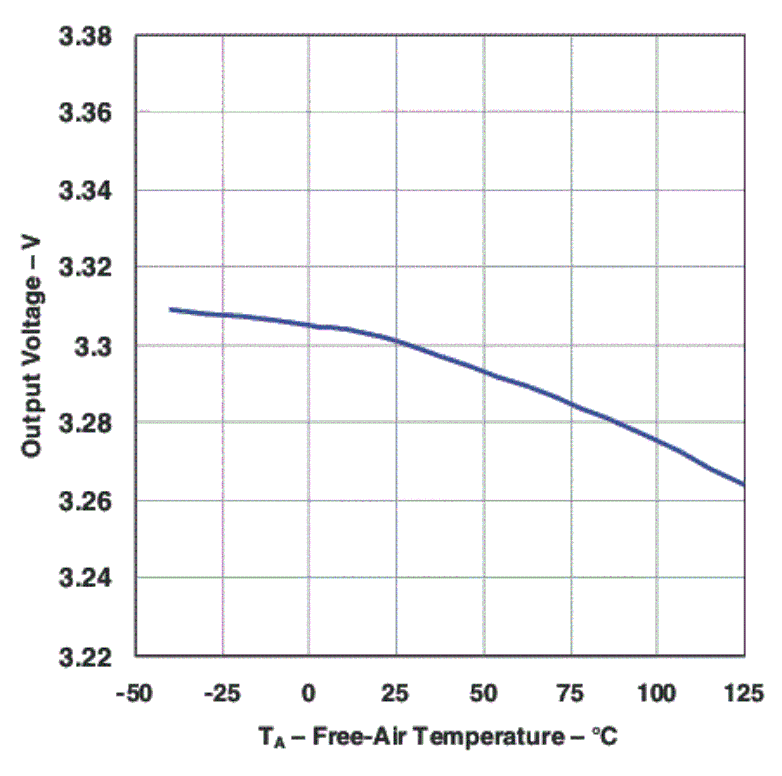
| IOUT = 1 mA | TL1963A-33 |
| TJ = 25 °C | ROUT = 4.3kΩ | VSHDN = VIN |
| TJ = 25 °C | VOUT = 1.21 V | VSHDN = VIN |
| TJ = 25 °C | VSHDN = VIN |
| VSHDN = 0 V |
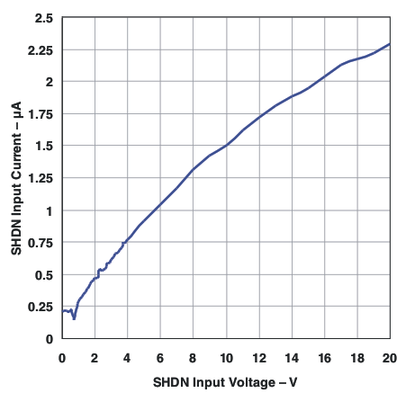 Figure 16. SHDN Pin Current (ISHDN) vs SHDN Input Voltage
| IOUT = 1 mA |
| ΔVOUT = 100 mV |
| TJ = 25 °C | VIN = 0 V | |
| Current flows into OUT pin | ||
| VRIPPLE = 0.05 VPP | CIN = 0 | TA = 25 °C |
| VIN = 2.7 V | COUT = 10 µF (ceramic) | |
| COUT = 10 µF (ceramic) | IOUT = 1.5 A |
| VIN = 4.3 V | CIN = 10 µF | |
| COUT = 10 µF (ceramic) | ||