SBVS237 March 2014 TLC5955
PRODUCTION DATA.
- 1 Features
- 2 Applications
- 3 Description
- 4 Revision History
- 5 Terminal Configurations and Functions
- 6 Specifications
- 7 Parameter Measurement Information
-
8 Detailed Description
- 8.1 Overview
- 8.2 Functional Block Diagram
- 8.3 Feature Description
- 8.4 Device Functional Modes
- 9 Applications and Implementation
- 10Power Supply Recommendations
- 11Layout
- 12Device and Documentation Support
- 13Mechanical, Packaging, and Orderable Information
パッケージ・オプション
メカニカル・データ(パッケージ|ピン)
サーマルパッド・メカニカル・データ
発注情報
6 Specifications
6.1 Absolute Maximum Ratings(1)
Over operating free-air temperature range, unless otherwise noted.| MIN | MAX | UNIT | ||||
|---|---|---|---|---|---|---|
| VCC | Voltage(2) | Supply | –0.3 | +6.0 | V | |
| VIN | Input range | SIN, SCLK, LAT, GSCLK | –0.3 | VCC + 0.3 | V | |
| VOUT | Output range | SOUT | –0.3 | VCC + 0.3 | V | |
| OUTR0 to OUTR15, OUTG0 to OUTG15, OUTB0 to OUTB15 | –0.3 | +11 | V | |||
| TJ (max) | Maximum operating junction temperature | +150 | °C | |||
(1) Stresses beyond those listed under Absolute Maximum Ratings may cause permanent damage to the device. These are stress ratings only, and functional operation of the device at these or any other conditions beyond those indicated under Recommended Operating Conditions is not implied. Exposure to absolute-maximum-rated conditions for extended periods my affect device reliability.
(2) All voltages are with respect to device ground terminal.
6.2 Handling Ratings
| MIN | MAX | UNIT | ||
|---|---|---|---|---|
| TSTG | Storage temperature range | –55 | +150 | °C |
| VESD(1) | Human body model (HBM) ESD stress voltage(2) | 4000 | V | |
| Charged device model (CDM) ESD stress voltage(3) | 2000 | V |
(1) Electrostatic discharge (ESD) to measure device sensitivity and immunity to damage caused by assembly line electrostatic discharges in to the device.
(2) Level listed above is the passing level per ANSI, ESDA, and JEDEC JS-001. JEDEC document JEP155 states that 4000-V HBM allows safe manufacturing with a standard ESD control process.
(3) Level listed above is the passing level per EIA-JEDEC JESD22-C101. JEDEC document JEP157 states that 2000-V CDM allows safe manufacturing with a standard ESD control process.
6.3 Recommended Operating Conditions
| PARAMETER | TEST CONDITIONS | MIN | NOM | MAX | UNIT | |
|---|---|---|---|---|---|---|
| DC CHARACTERISTICS | ||||||
| VCC | Supply voltage | 3.0 | 5.5 | V | ||
| VO | Voltage applied to output | OUTX0 to OUTX15(2) | 10 | V | ||
| VIH | High-level input voltage | SIN, SCLK, LAT, GSCLK | 0.7 × VCC | VCC | V | |
| VIL | Low-level input voltage | SIN, SCLK, LAT, GSCLK | GND | 0.3 × VCC | V | |
| IOH | High-level output current | SOUT | –2 | mA | ||
| IOL | Low-level output current | SOUT | 2 | mA | ||
| IOLC | Constant output sink current | OUTX0 to OUTX15(2), 3 V ≤ VCC ≤ 3.6 V | 23.9 | mA | ||
| OUTX0 to OUTX15(2), 3.6 V < VCC ≤ 5.5 V | 31.9 | mA | ||||
| TA | Operating free-air temperature range | –40 | +85 | °C | ||
| TJ | Operating junction temperature range | –40 | +125 | °C | ||
| AC CHARACTERISTICS | ||||||
| fCLK (SCLK) | Data shift clock frequency | SCLK | 25 | MHz | ||
| fCLK (GSCLK) | Grayscale control clock frequency | GSCLK | 33 | MHz | ||
| tWH0 | Pulse duration | SCLK | 10 | ns | ||
| tWL0 | SCLK | 10 | ns | |||
| tWH1 | GSCLK | 10 | ns | |||
| tWL1 | GSCLK | 10 | ns | |||
| tWH2 | LAT | 30 | ns | |||
| tSU0 | Setup time | SIN to SCLK↑ | 5 | ns | ||
| tSU1 | LAT↓ to SCLK↑ (auto data refresh is disabled(1)) | 30 | ns | |||
| tSU2 | LAT↑ for GS data written to GSCLK↑ when display time reset mode is disabled | 50 | ns | |||
| tSU3 | LAT↑ for GS data written to GSCLK↑ when display time reset mode is enabled | 70 | ns | |||
| tH0 | Hold time | SCLK↑ to SIN | 2 | ns | ||
| tH1 | SCLK↑ to LAT↑ | 5 | ns | |||
(1) When auto data refresh is enabled, the first SCLK rising edge after the LAT signal input must be input after the first GSCLK is input.
(2) X = R, G, or B.
6.4 Thermal Information
| THERMAL METRIC(1) | DCA (HTSSOP) | RTQ (QFN) | UNIT | |
|---|---|---|---|---|
| 56 TERMINALS | 56 TERMINALS | |||
| θJA | Junction-to-ambient thermal resistance | 32.2 | 27.9 | °C/W |
| θJCtop | Junction-to-case (top) thermal resistance | 16.8 | 14.9 | |
| θJB | Junction-to-board thermal resistance | 16.1 | 6.5 | |
| ψJT | Junction-to-top characterization parameter | 0.8 | 0.3 | |
| ψJB | Junction-to-board characterization parameter | 16.0 | 6.4 | |
| θJCbot | Junction-to-case (bottom) thermal resistance | 0.9 | 2.0 | |
(1) For more information about traditional and new thermal metrics, see the IC Package Thermal Metrics application report, SPRA953.
6.5 Electrical Characteristics
At TA = –40°C to +85°C and VCC = 3 V to 5.5 V, unless otherwise noted. Typical values at TA = +25°C and VCC = 3.3 V.| PARAMETER | CONDITION | MIN | TYP | MAX | UNIT | ||
|---|---|---|---|---|---|---|---|
| VOH | High-level output voltage (SOUT) | IOH = –2 mA | VCC – 0.4 | VCC | V | ||
| VOL | Low-level output voltage (SOUT) | IOL = 2 mA | 0.4 | V | |||
| IIN | Input current (SIN, SCLK, LAT, GSCLK) |
VIN = VCC or GND | –1 | 1 | μA | ||
| ICC0 | Supply current (VCC) | SIN, SCLK, and LAT = GND, all OUTXn = off, GSCLK = GND, GSXn = 0000h, DCXn and BCX = 7Fh, VOUTXn = 0.8 V, MCX = 0 (3.2-mA target)(1)(2) |
15 | 20 | mA | ||
| ICC1 | SIN, SCLK, and LAT = GND, all OUTXn = off, GSCLK = GND, GSXn = 0000h, DCXn and BCX = 7Fh, VOUTXn = 0.8 V, MCX = 4 (19.1-mA target) |
16 | 22 | mA | |||
| ICC2 | SIN, SCLK, and LAT = GND, auto display repeat enabled, GSCLK = 33 MHz, GSXn = FFFFh, DCXn and BCX = 7Fh, VOUTXn = 0.8 V, MCX = 4 (19.1-mA target) | 18 | 26 | mA | |||
| ICC3 | VCC = 5.0 V, SIN, SCLK, and LAT = GND, auto display repeat enabled, GSCLK = 33 MHz, GSXn = FFFFh, DCXn and BCX = 7Fh, VOUTXn = 0.8 V, MCX = 7 (31.9-mA target) |
20 | 29 | mA | |||
| IOLC0 | Constant output sink current (OUTX0 to OUTX15) |
All OUTXn = on, DCXn and BCX = 7Fh, VOUTXn = VOUTfix = 0.8 V, MCX = 4 |
17.4 | 19.1 | 20.8 | mA | |
| IOLC1 | VCC = 5.0 V, all OUTXn = on, DCXn and BCX = 7Fh, VOUTXn = VOUTfix = 0.8 V, MCX = 7 | 29.1 | 31.9 | 34.7 | mA | ||
| IOLKG0 | Output leakage current (OUTX0 to OUTX15) |
All OUTn = off, VOUTXn = VOUTfix = 10 V, MCX = 7 |
TJ = +25°C | 0.1 | μA | ||
| IOLKG1 | TJ = +85°C | 0.2 | μA | ||||
| IOLKG2 | TJ = +125°C | 0.3 | 0.8 | μA | |||
| ΔIOLC0 | Constant-current error (channel-to-channel, OUTX0 to OUTX15)(3) |
All OUTXn = on, DCXn and BCX = 7Fh, VOUTXn = VOUTfix = 0.8 V, MCX = 4 |
±2% | ±5% | |||
| ΔIOLC1 | Constant-current error (device-to-device, OUTX0 to OUTX15)(4) |
All OUTXn = on, DCXn and BCX = 7Fh, VOUTXn = VOUTfix = 0.8 V, MCX = 4 |
±2% | ±4% | |||
| ΔIOLC2 | Line regulation (OUTx0 to OUTx15)(5) |
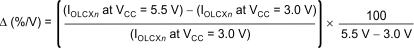
VCC = 3.0 V to 5.5 V, all OUTXn = on, DCXn and BCX = 7Fh, VOUTXn = VOUTfix = 0.8 V, MCX = 4 |
±0.1 | ±1 | %/V | ||
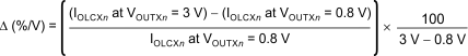
| ΔIOLC3 | Load regulation (OUTx0 to OUTx15)(6) |
All OUTXn = on, DCXn and BCX = 7Fh, VOUTXn = 0.8 V to 3.0 V, VOUTfix = 0.8 V, MCX = 4 |
±0.1 | ±1 | %/V | ||
| VLOD | LED open-detection threshold | All OUTXn = on | 0.25 | 0.30 | 0.35 | V | |
| VLSD0 | LED short-detection threshold | All OUTXn = on, LSDVLT = 0 | 0.65 × VCC | 0.70 × VCC | 0.75 × VCC | V | |
| VLSD1 | All OUTXn = on, LSDVLT = 1 | 0.85 × VCC | 0.90 × VCC | 0.95 × VCC | V | ||
(1) X = R, G, or B. For example, MCX = MCR, MCG, and MCG.
(2) n = 0 to 15.
(3) The deviation of each output from the OUTX0 to OUTX15 constant-current average of the same color group. Deviation is calculated by the formula:
where X = R, G, or B; n = 0 to 15.
where X = R, G, or B; n = 0 to 15.
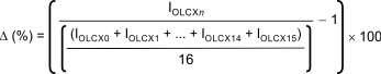
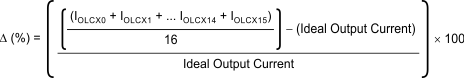
(4) Deviation of the OUTX0 to OUTX15 constant-current average from the ideal constant-current value.
Deviation is calculated by the formula:
where X = R, G, or B; n = 0 to 15.
Ideal current is the target current when MC is 4.
Deviation is calculated by the formula:
where X = R, G, or B; n = 0 to 15.
Ideal current is the target current when MC is 4.
(5) Line regulation is calculated by the formula:
where X = R, G, or B; n = 0 to 15.
where X = R, G, or B; n = 0 to 15.
(6) Load regulation is calculated by the equation:
where X = R, G, or B; n = 0 to 15.
where X = R, G, or B; n = 0 to 15.
6.6 Switching Characteristics
At TA = –40°C to +85°C, VCC = 3 V to 5.5 V, CL = 15 pF, RL = 120 Ω, MCX = 7, and VLED = 4.5 V, unless otherwise noted. Typical values at TA = +25°C and VCC = 3.3 V.| PARAMETER | TEST CONDITIONS | MIN | TYP | MAX | UNIT | ||
|---|---|---|---|---|---|---|---|
| tR0 | Rise time | SOUT | 3 | 5 | ns | ||
| tR1 | OUTXn, VCC = 3.6 V, DCXn, and BCX = 7Fh, TA = +25°C(2) | 30 | ns | ||||
| tF0 | Fall time | SOUT | 3 | 5 | ns | ||
| tF1 | OUTXn, VCC = 3.6 V, DCXn, and BCX = 7Fh, TA = +25°C | 40 | ns | ||||
| tD0 | Propagation delay | SCLK↑ to SOUT↑↓ | 20 | 30 | ns | ||
| tD1 | VCC = 3.6 V, GSCLK = 33 MHz, DCXn and BCX = 7Fh, TA = +25°C | GSCLK↑ to OUTX4 and OUTX11 on or off |
40 | ns | |||
| tD2 | GSCLK↑ to OUTX0 and OUTX15 on or off |
43 | ns | ||||
| tD3 | GSCLK↑ to OUTX5 and OUTX10 on or off |
46 | ns | ||||
| tD4 | GSCLK↑ to OUTX1 and OUTX14 on or off |
49 | ns | ||||
| tD5 | GSCLK↑ to OUTX2 and OUTX13 on or off |
52 | ns | ||||
| tD6 | GSCLK↑ to OUTX6 and OUTX9 on or off |
55 | ns | ||||
| tD7 | GSCLK↑ to OUTX3 and OUTX12 on or off |
58 | ns | ||||
| tD8 | GSCLK↑ to OUTX7 and OUTX8 on or off |
61 | ns | ||||
| tON_ERR | Output on-time error(1) | tOUTON – tGSCLK, VCC = 3.6 V to 5.5 V, GSXn = 0001h, GSCLK = 33 MHz, DCXn and BCX = 7Fh |
–20 | 20 | ns | ||
(1) Output on-time error (tON_ERR) is calculated by the formula: tON_ERR = tOUT_ON – tGSCLK. tOUTON is the actual on-time of the constant-current driver. tGSCLK is the GSCLK period.
(2) X = R, G, or B; n = 0 to 15.
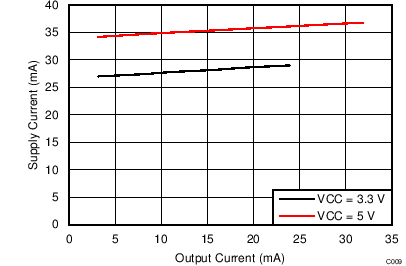
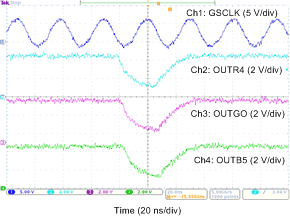
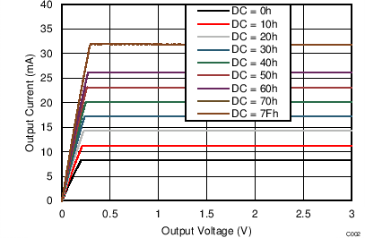
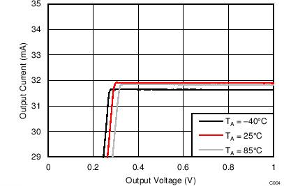
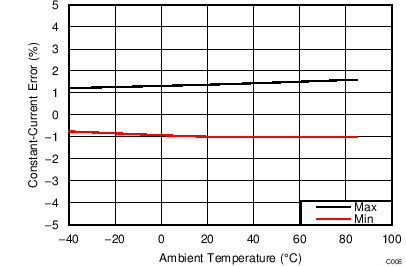
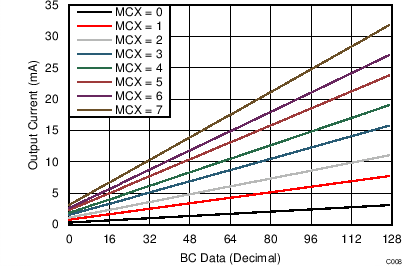
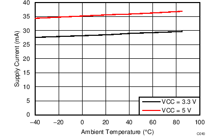
6.7 Typical Characteristics
At TA = +25°C and VCC = 5.0 V, unless otherwise noted.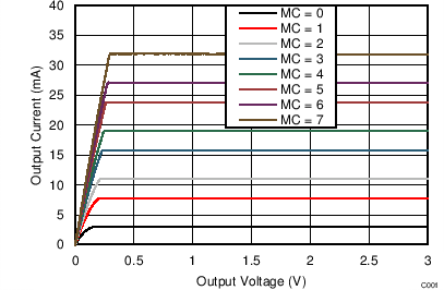
| BCX = DCXn = 7Fh |
(MCX Changing)
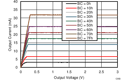
| BCX = DCXn = 7Fh |
(BCX Changing)
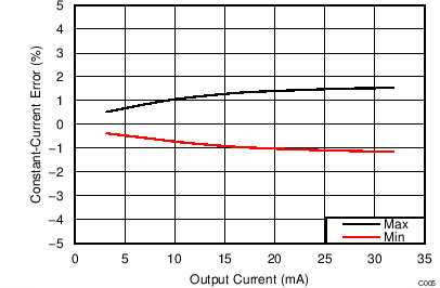
| BCX = DCXn = 7Fh | VOUTXn = 0.8 V | |
| BCX = 7Fh | VOUTXn = 0.8 V | |
| BCX = DCXn = 7Fh | SIN = 12.5 MHz | SCLK = 25 MHz |
| GSCLK = 33 MHz | VOUT = 0.8 V | GSXn = FFFFh |
| MCX = 7 | BCX = DCXn = 7Fh | GSCLK = 33 MHz | |||
| VLED = 4.5 V | RL = 120 Ω | GSXn = 0001h | |||
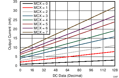
| BCX = DCXn = 7Fh |
(DCXn Changing)
| BCX = DCXn = 7Fh |
| MCX = 4 | BCX = DCXn = 7Fh | VOUTXn = 0.8 V |
| DCXn = 7Fh | VOUTXn = 0.8 V | |
| MCX = 4 | BCX = DCXn = 7Fh | SIN = 12.5 MHz |
| SCLK = 25 MHz | GSCLK = 33 MHz | VOUT = 0.8 V |
| GSXn = FFFFh |