JAJSCN6A November 2016 – May 2018 TLV170 , TLV2170 , TLV4170
PRODUCTION DATA.
- 1 特長
- 2 アプリケーション
- 3 概要
- 4 改訂履歴
- 5 Pin Configuration and Functions
- 6 Specifications
- 7 Detailed Description
- 8 Application and Implementation
- 9 Power Supply Recommendations
- 10Layout
- 11デバイスおよびドキュメントのサポート
- 12メカニカル、パッケージ、および注文情報
パッケージ・オプション
メカニカル・データ(パッケージ|ピン)
サーマルパッド・メカニカル・データ
- D|8
発注情報
8.2.2 Detailed Design Procedure
Figure 30 shows a unity-gain buffer driving a capacitive load. Equation 1 shows the transfer function for the circuit in Figure 30. Not shown in Figure 30 is the open-loop output resistance of the op amp, Ro.

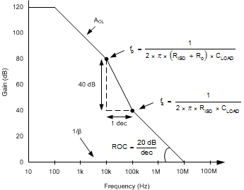
The transfer function in Equation 1 has a pole and a zero. The frequency of the pole (fp) is determined by (Ro + RISO) and CLOAD. Components RISO and CLOAD determine the frequency of the zero (fz). A stable system is obtained by selecting RISO such that the rate of closure (ROC) between the open-loop gain (AOL) and 1/β is 20 dB per decade; see Figure 31. The 1/β curve for a unity-gain buffer is 0 dB.
 Figure 31. TIPD128 Unity-Gain Amplifier With RISO Compensation
 ROC stability analysis is typically simulated. The validity of the analysis depends on multiple factors, especially the accurate modeling of Ro. In addition to simulating the ROC, a robust stability analysis includes a measurement of overshoot percentage and ac gain peaking of the circuit using a function generator, oscilloscope, and gain and phase analyzer. Phase margin is then calculated from these measurements. Table 4 shows the overshoot percentage and ac gain peaking that correspond to phase margins of 45° and 60°. For more details on this design and other alternative devices that can be used in place of the TLV170, see the Capacitive Load Drive Solution Using an Isolation Resistor precision design.
Table 4. Phase Margin versus Overshoot and AC Gain Peaking
| PHASE MARGIN | OVERSHOOT | AC GAIN PEAKING |
|---|---|---|
| 45° | 23.3% | 2.35 dB |
| 60° | 8.8% | 0.28 dB |