SLAS579A April 2009 – June 2015 TLV2553-Q1
PRODUCTION DATA.
- 1 Features
- 2 Applications
- 3 Description
- 4 Revision History
- 5 Pin Configuration and Functions
-
6 Specifications
- 6.1 Absolute Maximum Ratings
- 6.2 ESD Ratings
- 6.3 Recommended Operating Conditions
- 6.4 Thermal Information
- 6.5 Electrical Characteristics
- 6.6 External Reference Specifications
- 6.7 Operating Characteristics
- 6.8 Timing Requirements, VREF+ = 5 V
- 6.9 Timing Requirements, VREF+ = 2.5 V
- 6.10 Typical Characteristics
- 7 Parameter Measurement Information
-
8 Detailed Description
- 8.1 Overview
- 8.2 Functional Block Diagram
- 8.3 Feature Description
- 8.4 Device Functional Modes
- 9 Application and Implementation
- 10Power Supply Recommendations
- 11Layout
- 12Device and Documentation Support
- 13Mechanical, Packaging, and Orderable Information
パッケージ・オプション
メカニカル・データ(パッケージ|ピン)
サーマルパッド・メカニカル・データ
- PW|20
発注情報
7 Parameter Measurement Information
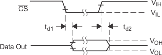 |
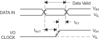 Figure 26. DATA IN and I/O CLOCK Voltage Figure 26. DATA IN and I/O CLOCK Voltage
|
 Waveforms |
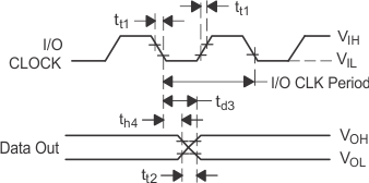 Figure 28. I/O CLOCK and DATA OUT Voltage Waveforms Figure 28. I/O CLOCK and DATA OUT Voltage Waveforms
|
 Figure 29. I/O CLOCK and EOC Voltage Waveforms Figure 29. I/O CLOCK and EOC Voltage Waveforms
|
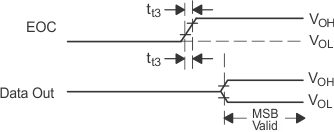 Figure 30. EOC and DATA OUT Voltage Waveforms Figure 30. EOC and DATA OUT Voltage Waveforms
|
 Figure 31. CS and EOC Waveforms Figure 31. CS and EOC Waveforms
|
 Figure 32. I/O CLOCK and DATA OUT Voltage Figure 32. I/O CLOCK and DATA OUT Voltage
|
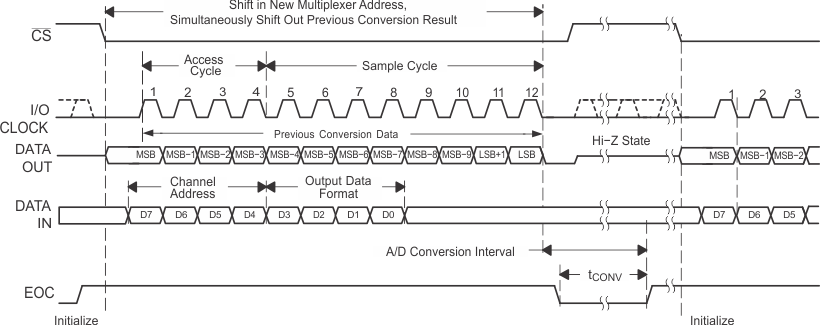 Figure 33. Timing for 12-Clock Transfer Using CS With DATA OUT Set for MSB First
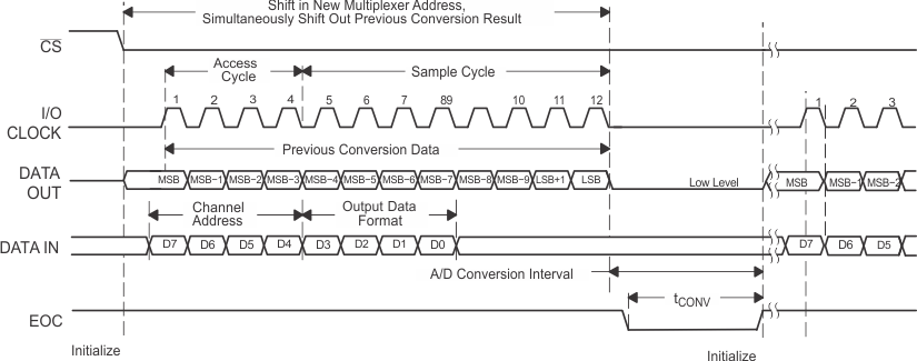
NOTE:
To minimize errors caused by noise at CS, the internal circuitry waits for a setup time after the CS falling edge before responding to control input signals. Therefore, no attempt should be made to clock in an address until the minimum CS setup time has elapsed.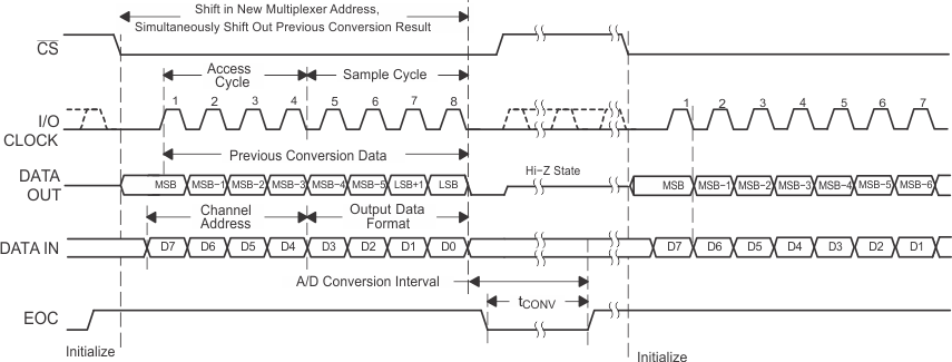 Figure 35. Timing for 8-Clock Transfer Using CS With DATA OUT Set for MSB First
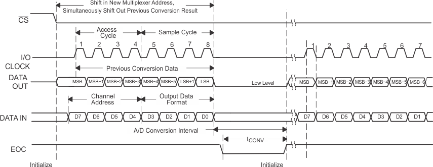
NOTE:
To minimize errors caused by noise at CS, the internal circuitry waits for a setup time after the CS falling edge before responding to control input signals. Therefore, no attempt should be made to clock in an address until the minimum CS setup time has elapsed.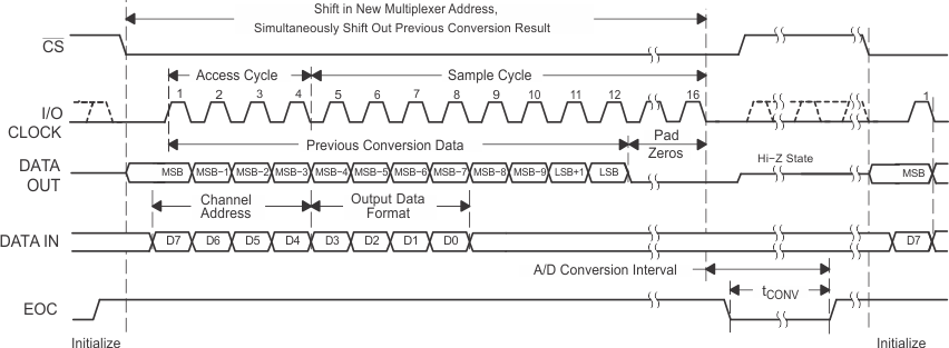 Figure 37. Timing for 16-Clock Transfer Using CS With DATA OUT Set for MSB First
NOTE:
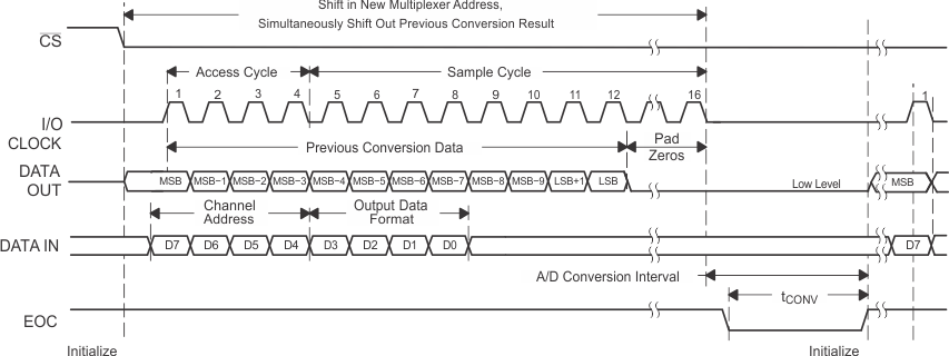
To minimize errors caused by noise at CS, the internal circuitry waits for a setup time after the CS falling edge before responding to control input signals. Therefore, no attempt should be made to clock in an address until the minimum CS setup time has elapsed.