JAJSN62C february 2004 – april 2023 TLV3011 , TLV3011B , TLV3012 , TLV3012B
PRODUCTION DATA
- 1 特長
- 2 アプリケーション
- 3 概要
- 4 Revision History
- 5 Pin Configuration and Functions
-
6 Specifications
- 6.1 Absolute Maximum Ratings- TLV3011 and TLV3012
- 6.2 Absolute Maximum Ratings - TLV3011B and TLV3012B
- 6.3 ESD Ratings
- 6.4 Thermal Information - TLV3011 and TLV3012
- 6.5 Thermal Information- TLV3011B and TLV3012B
- 6.6 Recommended Operating Conditions
- 6.7 Electrical Characteristics - TLV3011 and TLV3012
- 6.8 Switching Characteristics - TLV3011 and TLV3012
- 6.9 Electrical Characteristics - TLV3011B and TLV3012B
- 6.10 Switching Characteristics - TLV3011B and TLV3012B
- 7 Typical Characteristics - TLV3011 and TLV3012
- 8 Typical Characteristics - TLV3011B and TLV3012B
- 9 Detailed Description
- 10Application and Implementation
- 11Device and Documentation Support
- 12Mechanical, Packaging, and Orderable Information
パッケージ・オプション
メカニカル・データ(パッケージ|ピン)
サーマルパッド・メカニカル・データ
- DCK|6
発注情報
10.2.1.2 Detailed Design Procedure
Configure the circuit as shown in Figure 10-3. Connect (V+) to VBAT which also powers the microcontroller. Resistors R1 and R2 create the under-voltage alert level of 2.0 V. When the battery voltage sags down to 2.0 V, the resistor divider voltage crosses VREF, the 1.242 V reference threshold of the TLV3012. This causes the comparator output to transition from a logic high to a logic low. The push-pull output of the TLV3012 is selected since the comparator operating voltage is shared with the microcontroller which is receiving the under-voltage alert signal.
Equation 2 is derived from the analysis of Figure 10-3.
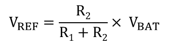
where
- R1 and R2 are the resistor values for the resistor divider connected to IN+
- VBAT is the voltage source that is being monitored for an undervoltage condition.
- VREF is the falling edge threshold where the comparator output changes state from high to low
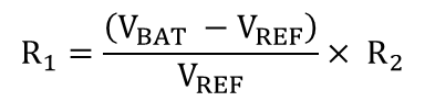
Rearranging Equation 2 and solving for R1 yields Equation 3.
For the specific undervoltage detection of 2.0 V using the TLV3012, the following results are calculated.
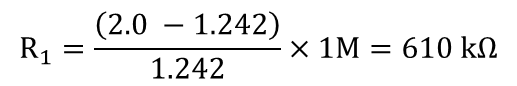
where
- R2 is set to 1 MΩ
- VBAT is set to 2.0 V
- VREF is set to1.242 V
Choose RTOTAL (R1 + R2) such that the current through the divider is at least 100 times higher than the input bias current (IBIAS). The resistors can have high values to minimize current consumption in the circuit without adding significant error to the resistive divider.