JAJSCS9B November 2016 – August 2017 TLV2316-Q1 , TLV316-Q1 , TLV4316-Q1
PRODUCTION DATA.
- 1 特長
- 2 アプリケーション
- 3 概要
- 4 改訂履歴
- 5 Device Comparison Table
- 6 Pin Configuration and Functions
- 7 Specifications
- 8 Detailed Description
- 9 Application and Implementation
- 10Power Supply Recommendations
- 11Layout
- 12デバイスおよびドキュメントのサポート
- 13メカニカル、パッケージ、および注文情報
6 Pin Configuration and Functions
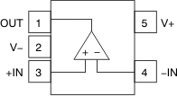
TLV316-Q1 DBV Package
5-Pin SOT-23
Top View

Pin Functions: TLV316-Q1
| PIN | I/O | DESCRIPTION | |
|---|---|---|---|
| NAME | NO. | ||
| –IN | 4 | I | Inverting input |
| +IN | 3 | I | Noninverting input |
| OUT | 1 | O | Output |
| V– | 2 | — | Negative (lowest) supply or ground (for single-supply operation) |
| V+ | 5 | — | Positive (highest) supply |
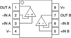
Pin Functions: TLV2316 -Q1
| PIN | I/O | DESCRIPTION | |
|---|---|---|---|
| NAME | NO. | ||
| –IN A | 2 | I | Inverting input, channel A |
| +IN A | 3 | I | Noninverting input, channel A |
| –IN B | 6 | I | Inverting input, channel B |
| +IN B | 5 | I | Noninverting input, channel B |
| OUT A | 1 | O | Output, channel A |
| OUT B | 7 | O | Output, channel B |
| V– | 4 | — | Negative (lowest) supply or ground (for single-supply operation) |
| V+ | 8 | — | Positive (highest) supply |
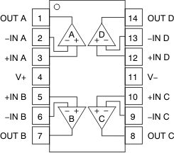
Pin Functions: TLV4316-Q1
| PIN | I/O | DESCRIPTION | |
|---|---|---|---|
| NAME | NO. | ||
| –IN A | 2 | I | Inverting input, channel A |
| +IN A | 3 | I | Noninverting input, channel A |
| –IN B | 6 | I | Inverting input, channel B |
| +IN B | 5 | I | Noninverting input, channel B |
| –IN C | 9 | I | Inverting input, channel C |
| +IN C | 10 | I | Noninverting input, channel C |
| –IN D | 13 | I | Inverting input, channel D |
| +IN D | 12 | I | Noninverting input, channel D |
| OUT A | 1 | O | Output, channel A |
| OUT B | 7 | O | Output, channel B |
| OUT C | 8 | O | Output, channel C |
| OUT D | 14 | O | Output, channel D |
| V– | 11 | — | Negative (lowest) supply or ground (for single-supply operation) |
| V+ | 4 | — | Positive (highest) supply |

