SLOS545D November 2008 – December 2014 TLV320AIC3107
UNLESS OTHERWISE NOTED, this document contains PRODUCTION DATA.
- 1 Features
- 2 Applications
- 3 Description
- 4 Simplified Block Diagram
- 5 Revision History
- 6 Description (Continued)
- 7 Pin Configuration and Functions
- 8 Specifications
- 9 Parameter Measurement Information
-
10Detailed Description
- 10.1 Overview
- 10.2 Functional Block Diagram
- 10.3
Feature Description
- 10.3.1 Hardware Reset
- 10.3.2 Digital Audio Data Serial Interface
- 10.3.3 Audio Data Converters
- 10.3.4 Audio Analog Inputs
- 10.3.5 Analog Line Output Drivers
- 10.3.6 Analog High Power Output Drivers
- 10.3.7 Input Impedance and VCM Control
- 10.3.8 General Purpose I/O
- 10.3.9 MICBIAS Generation
- 10.3.10 Class-D Speaker Driver
- 10.3.11 Short Circuit Output Protection
- 10.3.12 Jack and Headset Detection
- 10.4 Device Functional Modes
- 10.5 Programming
- 10.6 Register Maps
- 11Application and Implementation
- 12Power Supply Recommendations
- 13Layout
- 14Device and Documentation Support
- 15Mechanical, Packaging, and Orderable Information
パッケージ・オプション
メカニカル・データ(パッケージ|ピン)
サーマルパッド・メカニカル・データ
- RSB|40
発注情報
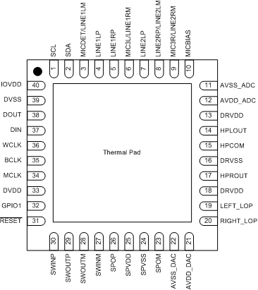
7 Pin Configuration and Functions
RSB Package
40-Pin WQFN With Exposed Thermal Pad
Bottom View
YZF Package
42-Pin DSBGA (6 × 7)
Bottom View
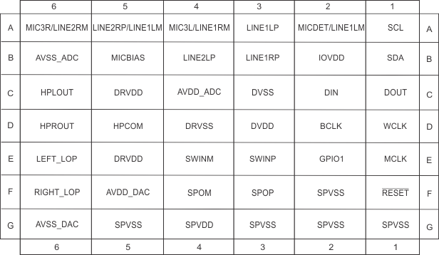
Pin Functions
| PIN | I/O | DESCRIPTION | ||
|---|---|---|---|---|
| QFN | WCSP(1) | NAME | ||
| 1 | A1 | SCL | I | I2C serial clock |
| 2 | B1 | SDA | I/O | I2C serial data input/output |
| 3 | A2 | MICDET/LINE1LM | I | MIC1 or Line1 analog input (left – or multifunctional) or Microphone detect |
| 4 | A3 | LINE1LP | I | MIC1 or Line1 analog input (left + or multifunctional) |
| 5 | B3 | LINE1RP | I | MIC1 or Line1 analog input (R + or multifunctional) |
| 6 | A4 | MIC3L/LINE1RM | I | MIC3 or Line1 analog input (R - or multifunctional) |
| 7 | B4 | LINE2LP | I | MIC2 or Line2 analog input (left + or multifunctional) |
| 8 | A5 | LINE2RP/LINE2LM | I | MIC2 or Line2 analog input (left + or right - or multifunctional) |
| 9 | A6 | MIC3R/LINE2RM | I | MIC3 or Line2 analog input (right + or multifunctional) |
| 10 | B5 | MICBIAS | O | Microphone bias voltage output |
| 11 | B6 | AVSS_ADC | G | ADC analog ground supply, 0 V |
| 12 | C4 | AVDD_ADC | P | ADC analog voltage supply, 2.7 V–3.6 V |
| 13 | C5 | DRVDD | P | High-power output driver analog voltage supply, 2.7 V–3.6 V |
| 14 | C6 | HPLOUT | O | High-power output driver (left +) |
| 15 | D5 | HPCOM | O | High-power output driver (left – or multifunctional) |
| 16 | D4 | DRVSS | G | High-power output driver analog ground supply, 0 V |
| 17 | D6 | HPROUT | O | High-power output driver (right +) |
| 18 | E5 | DRVDD | P | High-power output driver analog voltage supply, 2.7 V–3.6 V |
| 19 | E6 | LEFT_LOP | O | Left line output |
| 20 | F6 | RIGHT_LOP | O | Right line output |
| 21 | F5 | AVDD_DAC | P | DAC analog voltage supply, 2.7 V–3.6 V |
| 22 | G6 | AVSS_DAC | G | DAC analog ground supply, 0 V |
| 23 | F4 | SPOM | O | Class-D (or Bypass SW, WCSP only) negative differential output |
| 24 | F2, G1, G2, G3, G5 | SPVSS | G | Class-D ground supply, 0 V |
| 25 | G4 | SPVDD | P | Class-D voltage supply, 2.7 V–5.5 V |
| 26 | F3 | SPOP | O | Class-D (or Bypass SW, WCSP only) positive differential output |
| 27 | E4 | SWINM | I | Negative Bypass Switch Input |
| 28 | — | SWOUTM | O | Negative Bypass Switch Output, to be tied to SPOM externally |
| 29 | — | SWOUTP | O | Positive Bypass Switch Output, to be tied to SPOP externally |
| 30 | E3 | SWINP | I | Positive Bypass Switch Input |
| 31 | F1 | RESET | I | Reset |
| 32 | E2 | GPIO1 | I/O | General-purpose input/output |
| 33 | D3 | DVDD | P | Digital core voltage supply, 1.525 V–1.95 V |
| 34 | E1 | MCLK | I | Master clock input |
| 35 | D2 | BCLK | I/O | Audio serial data bus bit clock (input/output) |
| 36 | D1 | WCLK | I/O | Audio serial data bus word clock (input/output) |
| 37 | C2 | DIN | I | Audio serial data bus data input (input) |
| 38 | C1 | DOUT | O | Audio serial data bus data output (output) |
| 39 | C3 | DVSS | G | Digital core / I/O ground supply, 0 V |
| 40 | B2 | IOVDD | P | I/O voltage supply, 1.1 V–3.6 V |
(1) Product Preview