SLVS568D January 2005 – April 2016 TLV341 , TLV341A , TLV342 , TLV342S
PRODUCTION DATA.
- 1 Features
- 2 Applications
- 3 Description
- 4 Revision History
- 5 Pin Configuration and Functions
-
6 Specifications
- 6.1 Absolute Maximum Ratings
- 6.2 ESD Ratings
- 6.3 Recommended Operating Conditions
- 6.4 Thermal Information: TLV341
- 6.5 Thermal Information: TLV342
- 6.6 Thermal Information: TLV342S
- 6.7 Electrical Characteristics: V+ = 1.8 V
- 6.8 Electrical Characteristics: V+ = 5 V
- 6.9 Shutdown Characteristics: V+ = 1.8 V
- 6.10 Shutdown Characteristics: V+ = 5 V
- 6.11 Typical Characteristics
- 7 Detailed Description
- 8 Application and Implementation
- 9 Power Supply Recommendations
- 10Layout
- 11Device and Documentation Support
- 12Mechanical, Packaging, and Orderable Information
7 Detailed Description
7.1 Overview
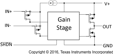
The TLV34xx devices are precision operational amplifiers with CMOS inputs for very low input bias current. Grade A devices offer lower VIO for high accuracy in direct-coupled applications. Output is rail to rail and input common mode includes ground. TLV341 and TLV342S have shutdown mode for very low supply current.
7.2 Functional Block Diagram

7.3 Feature Description
7.3.1 PMOS Input Stage
PMOS Input Stage supports a lower input range that includes ground. Upper range limit is VCC – 0.6 V.
7.3.2 CMOS Output Stage
The CMOS drain output topology allows rail-to-rail output swing.
7.3.3 Shutdown
TLV341 and TLV342S include a shutdown pin. During shutdown, ICC is nearly zero and the output becomes high impedance. The typical turnon time coming out of shutdown is 5 µs.
7.4 Device Functional Modes
The TLV34xx devices have two operation modes:
- Normal operation when SHDN pin is at V+ level or the SHDN pin is not present
- Shutdown mode when SHDN is at GND level; ICC is very low and output is high impedance.