JAJSC92D June 2016 – May 2017 TLV6001 , TLV6002 , TLV6004
PRODUCTION DATA.
- 1 特長
- 2 アプリケーション
- 3 概要
- 4 改訂履歴
- 5 Pin Configuration and Functions
-
6 Specifications
- 6.1 Absolute Maximum Ratings
- 6.2 ESD Ratings
- 6.3 Recommended Operating Conditions
- 6.4 Thermal Information: TLV6001
- 6.5 Thermal Information: TLV6002
- 6.6 Thermal Information: TLV6004
- 6.7 Electrical Characteristics: VS= 1.8 V to 5 V (±0.9 V to ±2.75 V)
- 6.8 Typical Characteristics: Table of Graphs
- 6.9 Typical Characteristics
- 7 Detailed Description
- 8 Application and Implementation
- 9 Power Supply Recommendations
- 10Layout
- 11デバイスおよびドキュメントのサポート
- 12メカニカル、パッケージ、および注文情報
パッケージ・オプション
メカニカル・データ(パッケージ|ピン)
- PW|14
サーマルパッド・メカニカル・データ
- PW|14
発注情報
8 Application and Implementation
NOTE
Information in the following applications sections is not part of the TI component specification, and TI does not warrant its accuracy or completeness. TI’s customers are responsible for determining suitability of components for their purposes. Customers should validate and test their design implementation to confirm system functionality.
8.1 Application Information
The TLV600x is a family of low-power, rail-to-rail input and output operational amplifiers specifically designed for portable applications. The devices operate from 1.8 V to 5.5 V, are unity-gain stable, and are suitable for a wide range of general-purpose applications. The class AB output stage is capable of driving ≤ 10-kΩ loads connected to any point between V+ and ground. The input common-mode voltage range includes both rails, and allows the TLV600x to be used in any single-supply application.
8.2 Typical Application
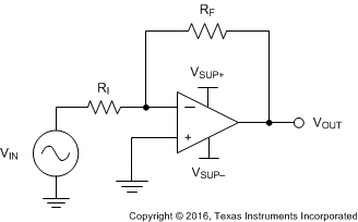
A typical application for an operational amplifier is an inverting amplifier, as shown in Figure 21. An inverting amplifier takes a positive voltage on the input and outputs a signal inverted to the input, making a negative voltage of the same magnitude. In the same manner, the amplifier makes negative input voltages positive on the output. In addition, amplification may be added by selecting the input resistor RI and the feedback resistor RF.
 Figure 21. Application Schematic
8.2.1 Design Requirements
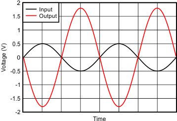
The supply voltage must be chosen to be larger than the input voltage range and the desired output range. The limits of the input common-mode range (VCM) and the output voltage swing to the rails (VO) must be considered. For instance, this application scales a signal of ±0.5 V (1 V) to ±1.8 V (3.6 V). Setting the supply at ±2.5 V is sufficient to accommodate this application.
8.2.2 Detailed Design Procedure
Determine the gain required by the inverting amplifier using Equation 1 and Equation 2:


When the desired gain is determined, choose a value for RI or RF. Choosing a value in the kilohm range is desirable for general-purpose applications because the amplifier circuit uses currents in the milliamp range. This milliamp current range ensures the device does not draw too much current. The trade-off is that large resistors (hundreds of kilohms) draw the smallest current but generate the highest noise. Small resistors (100s of ohms) generate low noise but draw high current. This example uses 10 kΩ for RI, meaning 36 kΩ is used for RF. The values are determined by Equation 3:

8.2.3 Application Curve
 Figure 22. Inverting Amplifier Input and Output
8.3 System Examples
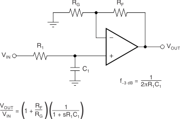
When receiving low-level signals, limiting the bandwidth of the incoming signals into the system is often required. The simplest way to establish this limited bandwidth is to place an RC filter at the noninverting terminal of the amplifier, as shown in Figure 23.
 Figure 23. Single-Pole Low-Pass Filter
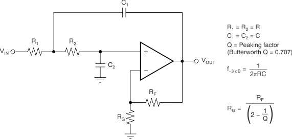
If even more attenuation is needed, a multiple pole filter is required. The Sallen-Key filter may be used for this task, as shown in Figure 24. For best results, the amplifier must have a bandwidth that is eight to 10 times the filter frequency bandwidth. Failure to follow this guideline may result in phase shift of the amplifier.
 Figure 24. Two-Pole, Low-Pass, Sallen-Key Filter