SBVS176B October 2011 – April 2016 TLV717P
PRODUCTION DATA.
- 1 Features
- 2 Applications
- 3 Description
- 4 Revision History
- 5 Pin Configuration and Functions
- 6 Specifications
- 7 Detailed Description
- 8 Application and Implementation
- 9 Power Supply Recommendations
- 10Layout
- 11Device and Documentation Support
- 12Mechanical, Packaging, and Orderable Information
パッケージ・オプション
メカニカル・データ(パッケージ|ピン)
- DQN|4
サーマルパッド・メカニカル・データ
- DQN|4
発注情報
8 Application and Implementation
NOTE
Information in the following applications sections is not part of the TI component specification, and TI does not warrant its accuracy or completeness. TI’s customers are responsible for determining suitability of components for their purposes. Customers should validate and test their design implementation to confirm system functionality.
8.1 Application Information
The TLV717P is a low-dropout regulator (LDO) with low quiescent current that delivers excellent line and load transient performance. This LDO regulator offers a foldback current limit. The operating junction temperature of this device series is –40°C to 85°C.
8.2 Typical Application
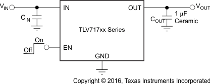
 Figure 15. Typical Application Circuit
8.2.1 Design Requirements
Table 2 lists the parameters for this application.
Table 2. Design Parameters
| PARAMETER | DESIGN REQUIREMENT |
|---|---|
| Input voltage | 3.8 V |
| Output voltage | 2.8 V ±1% |
| Output current | 30 to 150 mA |
8.2.2 Detailed Design Procedure
8.2.2.1 Input and Output Capacitor Requirements
TI recommends X5R- and X7R-type ceramic capacitors because they have minimal variation in value and equivalent series resistance (ESR) over temperature. The TLV717P is designed to be stable with an effective capacitance of 0.1 µF or larger at the output, though TI recommends a 1-µF ceramic capacitor for typical applications. Thus, the device is stable with capacitors of other dielectric types as well, as long as the effective capacitance under operating bias voltage and temperature is greater than 0.1 µF. This effective capacitance refers to the capacitance that the LDO detects under operating bias voltage and temperature conditions; that is, the capacitance after taking both bias voltage and temperature derating into consideration. In addition to allowing the use of cheaper dielectrics, this capability of being stable with 0.1-µF effective capacitance also enables the use of smaller footprint capacitors that have higher derating in size- and space-constrained applications. Using a 0.1-µF rated capacitor at the LDO output does not ensure stability because the effective capacitance under the specified operating conditions would be less than 0.1 µF. Maximum ESR should be less than 200 mΩ.
Although an input capacitor is not required for stability, it is good analog design practice to connect a 0.1-µF to 1-µF, low ESR capacitor across the IN and GND pins of the regulator. This capacitor counteracts reactive input sources and improves transient response, noise rejection, and ripple rejection. A higher-value capacitor may be necessary if large, fast, rise-time load transients are anticipated, or if the device is not located close to the power source. If source impedance is more than 2 Ω, a 0.1-µF input capacitor may be necessary to ensure stability.
8.2.2.2 Dropout Voltage
The TLV717P uses a PMOS pass transistor to achieve low dropout. When (VIN – VOUT) is less than the dropout voltage (VDO), the PMOS pass device is in the linear region of operation and the input-to-output resistance is the RDS(ON) of the PMOS pass element. VDO scales approximately with output current because the PMOS device behaves like a resistor in dropout. As with any linear regulator, PSRR and transient response are degraded as (VIN – VOUT) approaches dropout.
8.2.2.3 Transient Response
As with any regulator, increasing the size of the output capacitor reduces over- and undershoot magnitude but increases the duration of the transient response.
8.2.3 Application Curves

