JAJS306H August   2007  – December 2018 TMP102

PRODUCTION DATA.  

  1. 特長
  2. アプリケーション
    1.     概略回路図
  3. 概要
    1.     ブロック図
  4. 改訂履歴
  5. Pin Configuration and Functions
    1.     Pin Functions
  6. Specifications
    1. 6.1 Absolute Maximum Ratings
    2. 6.2 Handling Ratings
    3. 6.3 Recommended Operating Conditions
    4. 6.4 Thermal Information
    5. 6.5 Electrical Characteristics
    6. 6.6 Timing Requirements
    7. 6.7 Typical Characteristics
  7. Detailed Description
    1. 7.1 Overview
    2. 7.2 Functional Block Diagram
    3. 7.3 Feature Description
      1. 7.3.1  Digital Temperature Output
        1. Table 2. 12-Bit Temperature Data Format
      2. 7.3.2  Serial Interface
      3. 7.3.3  Bus Overview
      4. 7.3.4  Serial Bus Address
      5. 7.3.5  Writing and Reading Operation
      6. 7.3.6  Slave Mode Operations
        1. 7.3.6.1 Slave Receiver Mode
        2. 7.3.6.2 Slave Transmitter Mode
      7. 7.3.7  SMBus Alert Function
      8. 7.3.8  General Call
      9. 7.3.9  High-Speed (HS) Mode
      10. 7.3.10 Timeout Function
      11. 7.3.11 Timing Diagrams
    4. 7.4 Device Functional Modes
      1. 7.4.1 Continuos-Conversion Mode
      2. 7.4.2 Extended Mode (EM)
      3. 7.4.3 Shutdown Mode (SD)
      4. 7.4.4 One-Shot/Conversion Ready (OS)
      5. 7.4.5 Thermostat Mode (TM)
        1. 7.4.5.1 Comparator Mode (TM = 0)
        2. 7.4.5.2 Interrupt Mode (TM = 1)
    5. 7.5 Programming
      1. 7.5.1 Pointer Register
        1. Table 7. Pointer Addresses
      2. 7.5.2 Temperature Register
        1. Table 8. Byte 1 of Temperature Register
        2. Table 9. Byte 2 of Temperature Register
      3. 7.5.3 Configuration Register
        1. Table 10. Byte 1 of Configuration and Power-Up or Reset Format
        2. Table 11. Byte 2 of Configuration and Power-Up or Reset Format
        3. 7.5.3.1   Shutdown Mode (SD)
        4. 7.5.3.2   Thermostat Mode (TM)
        5. 7.5.3.3   Polarity (POL)
        6. 7.5.3.4   Fault Queue (F1/F0)
        7. 7.5.3.5   Converter Resolution (R1/R0)
        8. 7.5.3.6   One-Shot (OS)
        9. 7.5.3.7   EM Bit
        10. 7.5.3.8   Alert (AL Bit)
        11. 7.5.3.9   Conversion Rate (CR)
      4. 7.5.4 High- and Low-Limit Registers
        1. Table 13. Byte 1 Temperature Register HIGH
        2. Table 14. Byte 2 Temperature Register HIGH
        3. Table 15. Byte 1 Temperature Register LOW
        4. Table 16. Byte 2 Temperature Register LOW
  8. Application and Implementation
    1. 8.1 Application Information
    2. 8.2 Typical Application
      1. 8.2.1 Design Requirements
      2. 8.2.2 Detailed Design Procedure
      3. 8.2.3 Application Curve
  9. Power Supply Recommendations
  10. 10Layout
    1. 10.1 Layout Guidelines
    2. 10.2 Layout Example
  11. 11デバイスおよびドキュメントのサポート
    1. 11.1 ドキュメントのサポート
      1. 11.1.1 関連資料
    2. 11.2 ドキュメントの更新通知を受け取る方法
    3. 11.3 コミュニティ・リソース
    4. 11.4 商標
    5. 11.5 静電気放電に関する注意事項
    6. 11.6 Glossary
  12. 12メカニカル、パッケージ、および注文情報

パッケージ・オプション

メカニカル・データ(パッケージ|ピン)
サーマルパッド・メカニカル・データ
発注情報

Detailed Design Procedure

Place the TMP102 device in close proximity to the heat source that must be monitored, with a proper layout for good thermal coupling. This placement ensures that temperature changes are captured within the shortest possible time interval. To maintain accuracy in applications that require air or surface temperature measurement, care must be taken to isolate the package and leads from ambient air temperature. A thermally-conductive adhesive is helpful in achieving accurate surface temperature measurement.

The TMP102 device is a very low-power device and generates very low noise on the supply bus. Applying an RC filter to the V+ pin of the TMP102 device can further reduce any noise that the TMP102 device might propagate to other components. R(F) in Figure 15 must be less than 5 kΩ and C(F) must be greater than 10 nF.
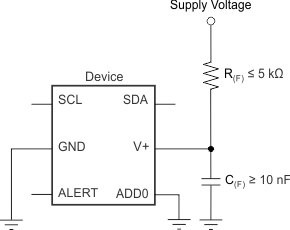
TMP102 ai_noise_slos887.gifFigure 15. Noise Reduction Techniques