JAJSJN1A May 2023 – September 2023 TMP4718
PRODUCTION DATA
- 1
- 1 特長
- 2 アプリケーション
- 3 概要
- 4 Revision History
- 5 Device Comparison
- 6 Pin Configuration and Functions
- 7 Specifications
-
8 Detailed Description
- 8.1 Overview
- 8.2 Functional Block Diagram
- 8.3
Feature Description
- 8.3.1 1.2-V Logic Compatible Inputs
- 8.3.2 Series Resistance Cancellation
- 8.3.3 Device Initialization, Resistor Decoding, and Default Temperature Conversion
- 8.3.4 Adjustable Default T_CRIT High-Temperature Limit
- 8.3.5 ALERT and T_CRIT Output
- 8.3.6 Fault Queue
- 8.3.7 Filtering
- 8.3.8 One-Shot Conversions
- 8.4 Device Functional Modes
- 8.5 Programming
- 8.6 Register Map
- 9 Application and Implementation
- 10Device and Documentation Support
- 11Mechanical, Packaging, and Orderable Information
8.3.7 Filtering
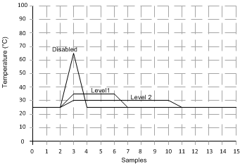
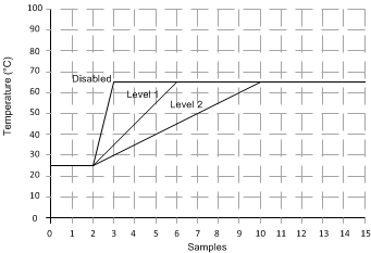
Remote junction temperature sensors are usually implemented in a noisy environment. Noise is most often created by fast digital signals that can corrupt measurements. A digital filter is available for the remote temperature measurements to reduce the effect of noise. This filter is programmable and has two levels when enabled. Level 1 performs a moving average of four consecutive samples. Level 2 performs a moving average of eight consecutive samples. The output of the digital filter is stored in the remote temperature result register, and the temperature limits are compared to this value. The filter responses to impulse and step inputs are shown in Figure 8-3 and Figure 8-4, respectively. The filter can be enabled or disabled by programming the desired levels in register settings. The digital filter is disabled by default.
The averages are cleared after the filter is set to 00h. Filtering can be used with both continuous conversions or one-shot conversions.
 Figure 8-3 Filter Response to Impulse
Inputs
 Figure 8-4 Filter Response to Step
Inputs
Figure 8-4 Filter Response to Step
InputsIn addition to the built-in digital filter of the device, TI recommends the user add an external capacitor between DP and DN pin on the remote channel. The capacitor acts as a bypass filter to help reduce high-frequency EMI noise when the device is operating in a noisy environment. The recommended optimal value for the capacitor is 470 pF and the value should not exceed 3 nF to allow proper operation of the temperature sensor.