SLOS313C December 2000 – March 2016 TPA6111A2
PRODUCTION DATA.
- 1 Features
- 2 Applications
- 3 Description
- 4 Revision History
- 5 Device Comparison Table
- 6 Pin Configuration and Functions
-
7 Specifications
- 7.1 Absolute Maximum Ratings
- 7.2 ESD Ratings
- 7.3 Recommended Operating Conditions
- 7.4 Thermal Information
- 7.5 DC Electrical Characteristics, VDD = 3.3 V
- 7.6 AC Operating Characteristics, VDD = 3.3 V
- 7.7 DC Electrical Characteristics, VDD = 5.5 V
- 7.8 AC Operating Characteristics, VDD = 5.5 V
- 7.9 AC Operating Characteristics, VDD = 3.3 V
- 7.10 AC Operating Characteristics, VDD = 5 V
- 7.11 Typical Characteristics
- 8 Parameter Measurement Information
- 9 Detailed Description
- 10Application and Implementation
- 11Power Supply Recommendations
- 12Layout
- 13Device and Documentation Support
- 14Mechanical, Packaging, and Orderable Information
パッケージ・オプション
デバイスごとのパッケージ図は、PDF版データシートをご参照ください。
メカニカル・データ(パッケージ|ピン)
- D|8
- DGN|8
サーマルパッド・メカニカル・データ
- DGN|8
発注情報
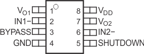
6 Pin Configuration and Functions
D or DGN Package
8-Pin SOIC or MSOP
Top View

Pin Functions
| PIN | I/O | DESCRIPTION | |
|---|---|---|---|
| NAME | NO. | ||
| BYPASS | 3 | I | Tap to voltage divider for internal mid-supply bias supply. Connect to a 0.1-µF to 1-µF low ESR capacitor for best performance. |
| GND | 4 | I | GND is the ground connection. |
| IN1– | 2 | I | IN1– is the inverting input for channel 1. |
| IN2– | 6 | I | IN2– is the inverting input for channel 2. |
| SHUTDOWN | 5 | I | Puts the device in a low quiescent current mode when held high |
| VDD | 8 | I | VDD is the supply voltage terminal. |
| VO1 | 1 | O | VO1 is the audio output for channel 1. |
| VO2 | 7 | O | VO2 is the audio output for channel 2. |