SLOS431B
March 2004 – February 2015
TPA6120A2
PRODUCTION DATA.
1
Features
2
Applications
3
Description
4
Simplified Schematic
5
Revision History
6
Pin Configuration and Functions
7
Specifications
7.1
Absolute Maximum Ratings
7.2
ESD Ratings
7.3
Recommended Operating Conditions
7.4
Thermal Information
7.5
Electrical Characteristics
7.6
Operating Characteristics
7.7
Typical Characteristics
8
Parameter Measurement Information
9
Detailed Description
9.1
Overview
9.2
Functional Block Diagram
9.3
Feature Description
9.3.1
Current-Feedback Amplifier
9.3.2
Independent Power Supplies
9.4
Device Functional Modes
10
Applications and Implementation
10.1
Application Information
10.2
Typical Application
10.2.1
High Voltage, High Fidelity DAC + Headphone Amplifier Solution
10.2.1.1
Design Requirements
10.2.1.2
Detailed Design Procedure
10.2.1.2.1
Resistor Values
10.2.1.2.2
Checking For Oscillations And Instability
10.2.1.2.3
Thermal Considerations
10.2.1.3
Application Performance Plots
10.2.2
High Fidelity Smartphone Application
10.2.2.1
Design Requirements
10.2.2.2
Detailed Design Procedure
10.2.2.3
Application Performance Plots
11
Power Supply Recommendations
11.1
Independent Power Supplies
11.2
Power Supply Decoupling
12
Layout
12.1
Layout Guidelines
12.2
Layout Example
13
Device and Documentation Support
13.1
Documentation Support
13.1.1
Related Documentation
13.2
Trademarks
13.3
Electrostatic Discharge Caution
13.4
Glossary
14
Mechanical, Packaging, and Orderable Information
パッケージ・オプション
デバイスごとのパッケージ図は、PDF版データシートをご参照ください。
メカニカル・データ(パッケージ|ピン)
RGY|14
DWP|20
サーマルパッド・メカニカル・データ
発注情報
slos431b_oa
slos431b_pm
8 Parameter Measurement Information
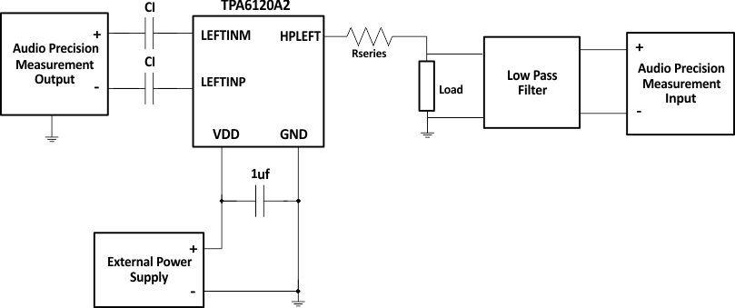
A. Separate power supply decoupling capacitors are used on all Vcc pins.
B. The low-pass filter is used to remove harmonic content above the audible range.
Figure 12. Test Circuit